


Recent Posts
Category
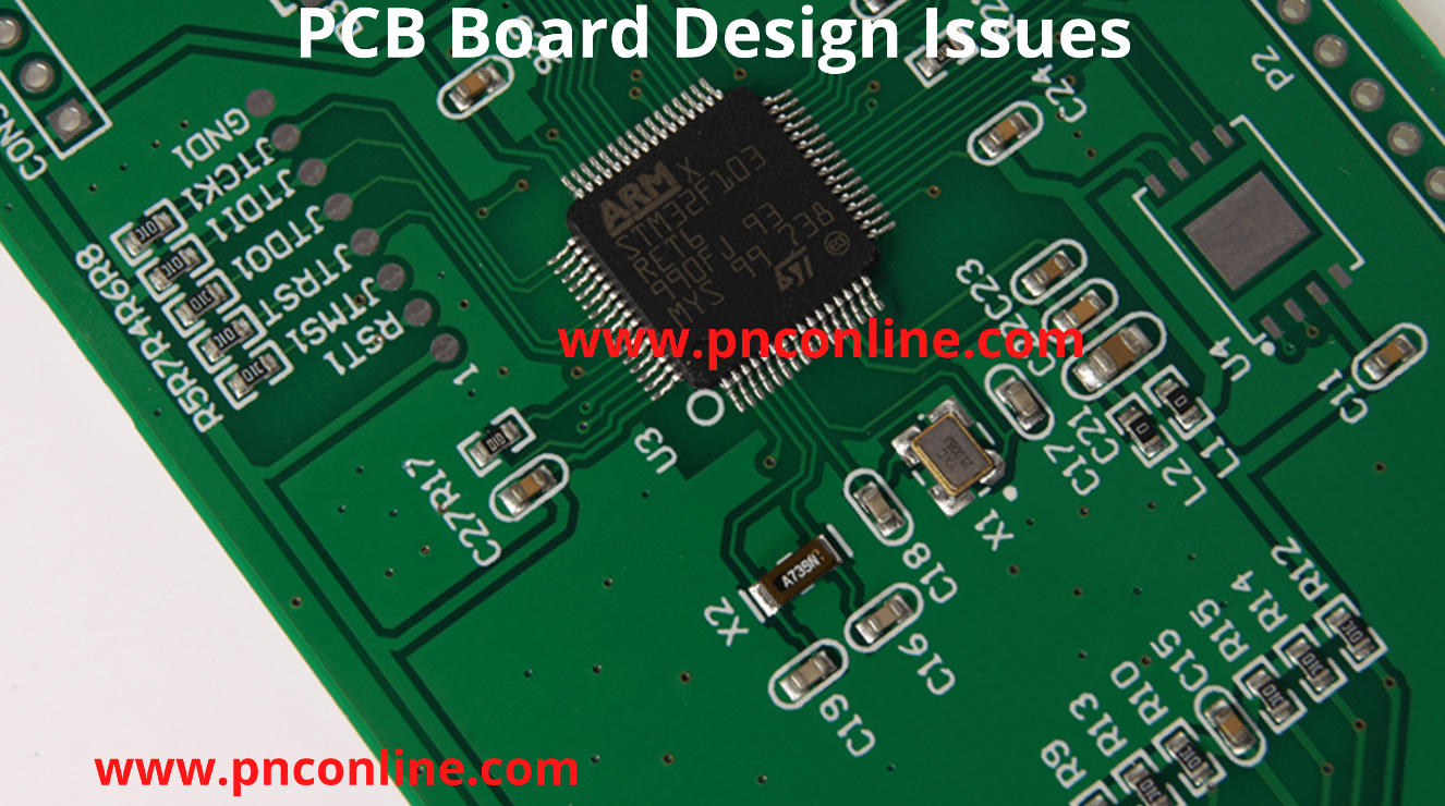
Printed Circuit Board Designing Issues
PCB’s play the role of heart and soul for any electronic device. This is the skeleton of any electronic device that applies to almost every field’s tools. Such as telecommunications, big to small computers, hardware, and military equipment. In a nutshell, you can say that an electronic device is completely dependent on its skeleton structure (in other words, on a printed circuit board) in order to perform well. As the PC board is the way to connect the within components as well as it maintains a healthy communication with the outside world so the electronic device can perform its functions, a simple or a slight mistake can lead to complete failure of the circuit or device and malfunction also.
It’s not an easy task to manage the designing of the circuit board, its internal associations, components, and layers. The chances of catastrophe and failure of the circuit are high when the layout design of the circuit is bad. Although the modern tools are assuring the innovative designs as compared to past designs. These tools also ensure the better design at the proper cost because in some cases, bad designing of the printed circuit board can lead to an expensive manufacturing process of the board. With that being said it is obvious that errors are more likely if the circuit designing is not done properly or in a timely. That’s the reason designing should be done on time before the manufacturing process. Reviewing the designing process before prototyping is also crucial.
Once the designs are reviewed independently then the prototyping process should come forward. This will reduce the overall cost of the manufacturing process as well as the failure of the circuit. We will discuss the common errors and design issues that occur during the process and lead to system failure. Moreover, in this article, we will discuss a few things that need to be kept in mind while designing a PCB for any circuit board manufacturer.
Some of the most common issues that happen during the manufacturing and designing process are discussed below.
The improper layout of circuit board:
As we know that devices are becoming smaller and smaller. This smaller requirement forces the combination of complex and thin development of the devices. Designers are also forced to make the design using smaller components and minimizing the distance between these components. Similarly, it is appreciated that minimal footprints are being used in the designing process. The smaller components used in designing reduce the footprints in the layout. For this purpose, a designer usually selects a layout in which components are placed very close. But this may result in an inefficient layout which further causes non-compliance and connection issues. The connection may go wrong in an incomplete layout. To get the desired functionality it is important that the defined layout of the circuit suits its needs also.
Moreover, the other thing that needs to be considered is that there should be enough space in the circuit to add some additional components or any other alternatives. If there is no need to add additional components, then these can always be removed before the manufacturing process takes place. So, a suitable and maintainable layout is required when you are working on high pin count and small pitch.
The decoupling capacitor is not in the right position:
There is no hard and fast definition that strictly explains the decoupling of capacitors. But for better understanding, we say that decoupling of a capacitor refers to the functionality of a capacitor in an electronic circuit. The decoupling capacitor maintains the stability of voltage in the circuit plane. So, in a designing process, a designer needs to make sure that capacitors are placed in the right position so that the transient or oscillation is providing enough power supply to all the other components of the board. For this purpose, the capacitor should be placed in a parallel position. It is also necessary that the position of the capacitor is as close to the components as possible in your PCB design.
The power source that provides the actual power must be properly routed on a printed circuit board for decoupling of the capacitor and the pin which requires a stable voltage supply. If a circuit is unable to do so, then decoupling of the capacitor cannot work properly. A series of inductors is also added if the circuit has some sensitive components such as analog to digital converter. In this case, the supply noise needs to be removed. This is done by using LC filters.
Antenna layout:
The antenna layout is one of the most critical tasks if your designed product is based on wireless technology. As this is the most critical part of the circuit board design, it is done incorrectly by common electrical engineers.
Also, transceivers transfer the maximum power between the antenna terminals when the impedance is matched perfectly. The impedance means the complexity of the circuit and not the simple resistance. The transceiver and the antenna can only be connected by a proper transmission line.
Mostly it is said that a 50-ohm impedance is enough in the transmission line for maximum power transfer in the antenna. The microstrip (having 50-ohm resistance) is used to attach both the transceiver and the antenna. Some free tools and calculators are there that can determine the printed circuit board transmission line dimension so that a user can achieve maximum and proper impedance. These tools are recommended if the designer is supposed to handle multiple types of transmission lines.
Acid Traps:
Acid trap used for the acute angles in the circuit board. These acute angles can trap acid in the etching process of printed circuit boards. These acute angles can place the acid in a specific corner for more than desired time and this results in eating more acid than intended. The circuit can become more defective and can cause a severe issue and the connection can be compromised.
This acid can also remove copper from the blackboard. Acid traps are commonly occurring problems are most designers are aware of them. That’s the reason. Designers are trained to avoid them also. But mistakes are always there to happen. Most of the time, acid trap errors happen because of human errors. And some software designs are also used to set the circuit if the setting is not done properly.
Acid traps can easily be caught in the second review of work, but oversight is possible. Moreover, the recent circuit tends to have less acid trap ratio than the previous ones because fabrication is switched by photo activated etching solution during the PC Board fabrication process.
Starved Thermal:
In the printed circuit board, the plane is connected to the pad by thermals. These pads are surrounded by thermals in the circuit. Thermals are an important component in the soldering process and are helpful for the pads in dispersing more heat effectively. But sometimes an error can happen because of an incomplete connection between thermal pads or the rest of the plane. This reduces the effective heat release or transfer by the system. And as a result, the circuit can catch various function problems. Starved thermal is a problem that does not allow the transfer of heat from the pad to the entire plane. This is more problematic if the circuit is under heat and in the soldering process. The assembly process will be slowed down and the pad will take more time to reflow and in heat transfer. In the end, the circuits having starved thermal can go through heat prone, insufficient heat transfer, and heat damages.
Starved thermal happens because of the defect present in the manufacturing process. These thermals are connected correctly in the computer-aided design system, but they have a weak connection with the entire plane board. This results in over machining and improper modeling in the circuit. The problem can be solved by replacing the thermal, but this is time-consuming and cost-consuming. But these thermals can be spotted before they make severe damage to the circuit.
Silvers:
Some narrow wages of copper and silver are used in printed circuit board manufacturing and can cause some serious problems during PCB manufacturing. These silvers occur in one or two ways and are produced in the etching process. The first way to produce silver is by etching the long thin feature of copper and solder mask.
On the other hand, silver can also be produced when a section of the printed circuit board is cut down too low or too deeply. The only way to reduce silver is to avoid the chance of producing them. The section width should be minimum. The producer can check the silvering defect by DFM.
These were just a few issues that commonly happen during printed circuit board designing and can be checked by the manufacturing committee. But sometimes, these issues have been overlooked that cause the problem in the end. The functionality of the circuit board fails, and the company and the user have to pay the cost for it. The only way to avoid these issues is by understanding the design properly.
Get your PCB design sorted with PNC. PNC is providing a turnkey solution to sort all your PCB design issues under one roof. Just contact us now at sales@pnconline.com.
Written by Sam Sangani

Sam Sangani is the President & CEO of PNC Inc., a Nutley, NJ based Printed Circuit Board manufacturer. Sam graduated from L. D. Engineering College with a BS Degree in Mechanical Engineering. He also continued his education and graduated from Steven’s Institute of Technology where he acquired a Master’s degree in Computer Science.
After completion of his BS, Sam worked as a QC Manager, for Xerox, Romania and London. He was responsible for the Quality Control of Cable and Wire Harness imports from Romania. After completing his Master’s Degree, he worked as a Senior Programmer with IBM, Tucson, Arizona. Sam was responsible for leading the Mainframe System Programming Team.
In 1997, Sam acquired PNC INC., a Nutley, NJ based PC Board fabrication Shop. From 1997-2013, Sam has made tremendous improvements and changes within PNC INC., as he added many new Products and Technologies in PNC’s portfolio. With his proven track record and leadership, PNC has never had an unprofitable year and has continued its growth yearly since 1997.
His current responsibilities are Strategic Planning, Corporate Management, New Business Ventures, Sales & Marketing, Trade Shows, Professional Services and leading productive teams to achieve peak potential. He has also utilized Lean Management techniques which have built a foundation for PNC’s high-paced growth. Sam also enjoys real-estate investing, web design & SEO, trading stocks, options, futures and Forex markets.


