Tag Archives: PC board manufacturer

PCB Prototyping

PCB Prototyping- Best Practices for Fast and Accurate Results

When designing a printed circuit board the prototyping process is one of the most important steps. It’s essential to get it right the first time so that the end product meets all of your specifications. To ensure fast and accurate results in this case, you must follow certain best practices. From choosing the right design software to properly testing the boards, we’ll cover everything you need to know to get the most out of your PCB prototyping projects.

Use the Correct Board Material

When it comes to PCB prototyping, selecting the right board material is crucial. The type of material you choose can impact the board’s durability, and performance. Some materials are more prone to overheating or warping, while others may be more conductive or have better insulating properties.

One popular option for PCB prototyping is fiberglass. It is a relatively low-cost material and can provide good insulation properties. It is also ideal for single-sided boards. However, it may not be the best option for more complex designs.

For multi-layered boards, you may want to consider a material like FR4. This type of material is more expensive but provides better durability and stability, which is critical for high-performance circuit boards.

Before selecting your board material, you must consider the specifications of your design, including the application, environment, and electrical properties you require. Don’t be afraid to consult with PC Board experts to help determine which material is the best fit for your project.

Using the right board material is just one of the many best practices to consider when it comes to PCB prototyping. By following these tips, you can achieve faster, more accurate outcomes and set yourself up for success in your PCB design projects.

Invest in Quality Components

When it comes to circuit board prototyping, investing in high-quality components is crucial to achieving fast and accurate results. While it may be tempting to cut costs by using cheaper parts, this can lead to several issues down the line, from malfunctioning circuits to reduced durability.

Using quality components ensures that your circuit board will function properly and last longer, saving you time and money in the long run. You must find the components that have been tested and verified to meet industry standards and specifications.

Another benefit of using high-quality components is that they are less likely to fail during testing, reducing the need for repairs or replacements. This not only saves you time but also minimizes the risk of damaging other components or causing additional issues with the circuit board.

Make Sure Your Board Design is Complete and Accurate

Before starting your PCB prototyping project, you must ensure that your board design is complete and accurate. This step may seem obvious, but it is often overlooked, resulting in errors and the waste of time and money.

Start by double-checking your PCB design for errors, missing connections, or any other issues. Use reliable design software and go over your schematic and layout files thoroughly. Get a second pair of eyes to review your design before moving forward with prototyping.

Another best practice is to perform a Design Rule Check (DRC). This automated check ensures that your board meets the minimum manufacturing requirements. A DRC can identify potential errors, such as overlapping pads, inconsistent track widths, or drill holes that are too small or too close to each other.

If your board design has multiple layers, it is crucial to verify that your stack-up is correct and that the signal integrity is maintained. You can use a simulation tool to predict and optimize the electrical performance of your board.

Follow the Data Sheet

Following the datasheet is essential to achieving accurate and reliable results while PCB prototyping. The data sheet contains crucial information about the board’s electrical characteristics, material properties, and manufacturing specifications.

The data sheet typically contains the following information:

  • PCB layer stack-up and dimensions
  • Minimum and maximum board thickness
  • Trace and via size, spacing, and clearance
  • Impedance requirements
  • Material composition and properties
  • Surface finish options
  • Solder mask and silkscreen specifications
  • Thermal management guidelines

Such a practice can ensure that your PCB prototype meets the manufacturer’s specifications, as well as any relevant industry standards. Failure to follow the datasheet can result in design flaws, manufacturing errors, and functionality issues.

Moreover, you should communicate with your PCB manufacturer if you have any questions or concerns about the datasheet. A reputable manufacturer has a team of experts who can guide you throughout the prototyping process. So, following the datasheet is the best practice for fast and accurate PCB prototyping.

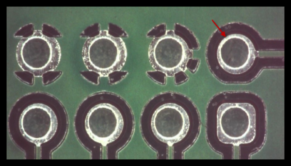
Make Test Points Accessible

Make sure that the test points are easily accessible. This helps have easy testing and debugging of the PCB during the prototype stage.

Test points are small metal points on the board where you can attach the testing equipment to measure the voltage. You can find them near components to be tested. By making them easily accessible, you can avoid having to take the board apart or maneuver equipment to access them. You should consider this factor during the design phase. Ideally, you should choose unobstructed areas. You should also consider adding extra test points to ensure thorough testing of the entire board.

Moreover, you should consider the size and type of test points to use. Small test points can be difficult to use, while larger test points can take up more space on the board. You should also consider the technology, such as surface mount or through-hole.

By making test points accessible during the prototyping phase, you can save time and ensure accurate results. It can also help to identify any issues with the board early on in the development process, helping in easier debugging and revisions.

Consider Your Assembly Options
After the PCB prototype process, comes the assembly. There are several assembly options available, and you should consider which one is best for your particular project.

One option is hand assembly, which involves soldering components to the board by hand. This method is cost-effective and works well for small-scale production runs, but it is time-consuming and may result in inconsistencies.

Another option is automated PCB assembly, which involves using machines to place components onto the board. This method is efficient and accurate, but it may be more expensive and more suitable for larger production runs.

You should also consider whether you want your board to be surface-mount or through-hole. Surface-mount components are smaller and lighter, making them ideal for compact designs. However, through-hole components can provide a stronger mechanical bond and are ideal for larger components or those that require high voltage.

Make sure to consider the assembly options before finalizing your PCB design and prototyping process. This will help ensure that the end product meets your expectations and requirements.

Don’t Forget the Silkscreen

When it comes to printed circuit board prototyping, people often overlook the importance of the silkscreen. The silkscreen is the layer of ink on top of the PCB that indicates component placement, orientation, and other important information. It may seem like a minor detail, but an accurate silkscreen can save a lot of time and confusion during the assembly process.

First and foremost, make sure your silkscreen is complete. This means double-checking that all component labels are correct and aligned properly with their respective pads. Make sure there are no overlapping labels or missing information.

Next, consider the size and color of the silkscreen. A too-small or too-light font may be difficult to read, especially for those with vision impairments. Conversely, a font that is too large or too dark can clutter the board.

Finally, be mindful of the placement of the silkscreen. It should not cover up any important traces or pads. Besides, it should not interfere with any assembly processes or inspection.

Final Thoughts

Prototyping printed circuit boards is a complex and time-consuming process, but with the right techniques, it doesn’t have to be. If you want to ensure fast and accurate results, you must follow best practices, in this case. Investing in quality components is an essential step in achieving fast and accurate PCB prototyping outcomes. Don’t compromise on quality to save a few bucks as it will end up costing you more in the long run. Also, make sure that your board design is complete and accurate, as it will save you time and money.

Before starting your PCB prototype, you should thoroughly review and understand the data sheet provided by the manufacturer. It ensures that your design meets the manufacturer’s specifications and industry standards, preventing errors and functionality issues. Also, don’t hesitate to consult with your prototype pcb manufacturer if you have any concerns about the datasheet.

Also, remember the importance of the silkscreen when prototyping your PCB. A well-designed silkscreen can improve the overall functionality and aesthetics of the PCB. Make sure to choose the right font and color, and be mindful of placement. A little attention to detail can go a long way in the success of your PCB prototyping project.

Would like to know more about PCB prototyping or printed circuit board assembly? Email us at sales@pnconline.com

Printed Circuit Board

Printed Circuit Board Backplane

Backplane PCBs are an essential component of many electrical systems, providing a convenient and efficient way to connect multiple printed circuit boards. We’ll explore the basics of backplane PCBs and discuss the process of fabricating them. Backplane PCBs vary in terms of types, construction materials, and the key steps in the fabrication process. After understanding all essentials, you can create a reliable, high-quality backplane Printed Circuit Board that meets your needs.

What is a Backplane PCB?

A backplane PCB, also known as a printed circuit board, is an interconnecting circuit board that helps support and provide electrical connections for multiple electronic components. The backplane PC Board provides a platform for connecting the individual PCBs that make up a larger electronic system. You can find the backplane PCBs in computers, servers, network switches, and routers.

The construction of backplane PCBs involves several layers of copper foil laminated together with an insulating material, such as glass-reinforced epoxy or polyimide. This combination of materials allows the backplane to be very durable and reliable. The copper traces that make up the interconnections are placed in specific patterns to create a flexible platform that can support various types of components.

Engineers use a backplane PCB to mount other types of PCBs, such as memory boards, processor boards, graphics cards, and storage devices. It also serves as a high-speed data bus between these components, providing faster communication and data transmission.

The Various Types of Backplane PCBs

Backplane PCBs come in a variety of shapes and sizes to meet the requirements of any design. These include double-sided, multilayer, surface mount, and rigid-flex backplanes. Each of these types offers distinct advantages and disadvantages, depending on the application.

Double-sided Backplane: This type of backplane has two layers of PCB material being connected by an array of holes drilled through the board. The application of this type of board is popular for low-cost, high-volume products such as consumer electronics.

Multilayer Backplane: This type of backplane has multiple layers of printed circuit board material being connected by various types of wiring. You will see its application in complex designs where routing or high density is essential.

Surface Mount Backplane: This type of backplane consists of one or more printed circuit boards with direct mounting onto the outside of another board. This type of board is suitable for high-speed applications, such as communication systems or computer networks.

Rigid-Flex Backplane: This type of backplane consists of two different printed circuit board materials. One layer is rigid and the other is flexible, allowing for greater flexibility in design. The board is ideal for applications with a large number of connections or tight spaces.

By understanding the different types of backplane PCBs, designers can choose the right type for their application and ensure that their product has the best performance possible.

Backplane PCB Fabrication
The fabrication of backplane PCBs involves a subtractive process, such as the removal of unwanted material from a starting substrate to create the desired traces and connections on the board. The most common method of fabrication is a chemical etching process, where manufacturers bond the copper foil onto the substrate, exposing it to a photoresist to create a pattern. The resist protects the copper during an acid etching step that removes the unwanted copper, leaving only the desired traces and connections. You can do it either manually or with an automated machine.

The complexity of the design and the number of layers will determine the board layout. The design is usually laid out in multiple layers, with each layer representing a different circuit or electrical signal. All the layers are then bonded together, creating the complete backplane PCB. The bonding of the layers involves either a chemical or thermal process, depending on the application.

After bonding the layers together, you may need to attach additional components to the board. This can include mounting holes for screws, heat sinks for components, and connectors for external devices. Then comes the typical process of components soldering onto the board, while keeping some in place with other methods such as rivets or adhesives.

In the end, you have to test it to make sure it works correctly. This includes electrical tests such as continuity tests and power tests to ensure that all the connections are working correctly. After thorough testing, the board is ready to use in its intended application.

The Advantages of Using a Backplane PCB

Backplane PCBs offer many advantages over traditional printed circuit boards They provide greater flexibility in terms of design and layout, as well as the ability to support larger numbers of components. This makes them ideal for high-density applications such as telecommunications, medical, industrial automation, and computing.

Using backplane PCBs also offers several other benefits. You can use them to reduce wiring complexity and cost since they allow for fewer wires in an interconnected system. Moreover, they make it easier to route signals and power within a device, allowing for more efficient communication between components. Besides, they help have the simultaneous operation of multiple cards or modules, which is beneficial in applications that require multiple functions.

Moreover, backplane PCB can also help reduce the size and weight of the final product. This is especially beneficial in applications that require a small form factor, such as portable electronics or embedded systems. Moreover, you can improve the overall reliability of the system due to the added strength of the backplane substrate.

The Disadvantages of Using a Backplane PCB

The main disadvantage of using a backplane PCB is its limited flexibility. Since all of the components are directly connected to the backplane, it can be difficult to modify or add new components to the board. This makes them less suitable for applications that require frequent changes or upgrades. Besides, they are more complex and costly to manufacture than other types of PCBs.

Another downside is that they take up a lot of space. Since they involve multiple layers, they require more physical area than simpler boards. This makes them less suitable for applications where size is an important factor. Besides, the wiring and component placement on a backplane PCB is quite challenging, since there are several connections to consider.

Moreover, backplane PCBs can also suffer from signal interference. This occurs when the signals from one component interfere with those from another component, leading to system errors or data corruption. This is especially true in the case of adjacent components with poor shielding.

Development Trend of Backplane

As technology advances, the need for higher performance and better reliability of backplane PCBs is on the rise. As a result, manufacturers are continuously developing new designs, materials, and components for backplane PCBs to ensure that they can keep up with the changing needs of the industry. The main trends in the development of backplane PCBs include miniaturization, increased functionality, improved signal integrity, and increased thermal efficiency.

Miniaturization: One of the main trends in the development of backplane PCBs is miniaturization. As more and more electronics are packed into smaller and smaller spaces, backplane PCBs should keep up with the trend. By reducing the size of the components used in the backplane, engineers can reduce the board area, allowing more components to fit into a smaller space.

Increased Functionality: As devices become increasingly complex, backplane PCBs must also provide more functionalities. By increasing the number of pins and features, engineers can provide more features in a single device. This helps engineers to design and develop more sophisticated products that can meet the needs of the market.

Improved Signal Integrity: To ensure reliable signal transmission, engineers must ensure that their backplane PCBs have good signal integrity. This involves optimizing the board layout, as well as using proper signal routing techniques. By improving signal integrity, engineers can reduce noise and the risk of data loss or interference from other signals.

Increased Thermal Efficiency: Heat management is essential for any electronic device, especially those containing multiple components. To ensure that the system is not facing high heat, backplane PCBs should be designed with thermal management in mind. By optimizing board layout and component placement, engineers can ensure a quick and effective dissipation of heat.

These are just some of the trends that are impacting backplane PCB design and development today. By incorporating these trends into their designs, engineers can create products to meet the ever-changing needs of the industry.

Final Thoughts

A backplane PCB, also known as a printed circuit board, is an interconnecting circuit board that helps support and provide electrical connections for multiple electronic components. The backplane PCB provides a platform for connecting the individual PCBs that make up a larger electronic system. You can find the backplane PCBs in computers, servers, network switches, and routers.

Engineers use a backplane PCB to mount other types of PCBs, such as memory boards, processor boards, graphics cards, and storage devices. It also serves as a high-speed data bus between these components, providing faster communication and data transmission. Certain development trends can help engineers create products to meet the ever-changing needs of the industry.

Would like to know more about the backplane PCBs or prototype pcb manufacturer? Email us at sales@pnconline.com

What is Printed Circuit Board Copper Clad Laminate?

What is Printed Circuit Board Copper Clad Laminate?

Printed circuit boards come in different materials known as substrate, including copper-clad laminate or CCL. PCB substrates are either organic or inorganic, depending on their properties. The organic substrates come up in different materials known as the reinforced board, such as glass felt, fiberglass, fiber paper, fiber cloth, and so on.
PCB fabricators impregnate there in forcing materials with an adhesive called resin, making it dry, and then cover it with copper foil at high pressure and temperature. Such a substrate is CCL or copper-clad laminate that resides on either one or both sides of the board. So, CCL is either single-sided or double-sided.
Rigid PCB has a rigid CCL with a substrate, such as

  • Resin epoxy FR4
  • PTFE
  • Aluminum or copper
  • Ceramic

These materials help make different types of PCBs, including single, double, and multilayer PCBs.

CCL Standards

Engineers define the CCL standard specification with ASTM D1867 and develop their circuit boards according to these standards. To cover twelve grades of CCL, ASTM needs the laminates to meet certain factors for peel strength, like

  • High temperatures
  • Volume resistivity
  • Water absorption
  • Flammability ratings
  • Dissipation
  • Dielectric breakdown
  • Permittivity
  • Lengthwise and crosswise strength

The PCB Manufacturer should also check the CCL for twist, warp, or blistering. CCL manufacturers often follow the IPC-410IC as a standard. Moreover, they use IPC-IM650 to test the fabricated CCL.

CCL Materials

FF4 CCL: As discussed above FR4 is a popular material for copper-clad laminate. The material is resin epoxy, and it is ideal for rigid circuit boards. You will see it on both sides and only one side of the board. The material is a combination of epoxy resin and fiberglass cloth. Resin makes the board fire resistant that’s why we abbreviate it as FR or flame retardant. However, it has to pass through testing to see if it is according to the UL94V-0 standards.

Copper base: like aluminum CCL, copper core CCL has a copper plate, copper foil, and dielectric layer for bonding. PCB’s thermal dissipation and dielectric bonding determine the overall thermal conductivity.
PCB with copper substrate has three types, depending on its design, such as copper without PTH, COB, or chip-on-board copper circuit board which is without the thermal pad insulation.
Aluminum CCL: Copper-clad laminate also has aluminum as a base material combined with a dielectric layer and copper foil. These materials are bonded through hot pressing and very high temperatures. The dielectric bonding determines the thermal conductivity of the aluminum core laminate. However, both copper foil and dielectric have high conductivity, and manufacturers often use ceramic to fill the dielectric layer.

What Is RF, Radio Frequency CCL?

The RF CCL is also known as the Microwave PC Board CCL as the board has microwave frequencies. Such a circuit board has certain characteristics to consider, such as

  • DK, dielectric constant
  • DF, dissipation factor
  • CTE, coefficient of thermal expansion
  • TCDR thermal coefficient of dielectric constant
  • Thermal conductivity

It involves high-frequency materials of which PTFE is a common practice. It is a synthetic material having great dielectric properties at high frequencies which are also known as microwave frequencies. A few companies develop the high-frequency PCB CCL, including Isola, Rogers, Taconic, and Panasonic.

What is Prepreg in CCL?

Prepreg or pre-impregnated CCL is a kind of fiberglass that is impregnated with a bonding material such as resin. The resin is not hard, however, it is dry and gets sticky when heated. In other words, the fiberglass is made strong through an adhesive just like FR4.
Prepreg materials come up in different thicknesses that determine their quality, such as standard resin, SR, medium resin, MR, or, high resin, HR. The PC Board manufacturer use the resin thickness according to the type of PCB they require.

What is Printed Circuit Board Copper Clad Laminate?
Printed Circuit Board Copper Clad Laminate

CCL PCB Applications

PCB with copper clad laminate is ideal for:

  • Electronics PCBs
  • Radars
  • High-speed communication devices, like 4G,5G, and LTE
  • Automotive products, such as ADAS radar
  • Avionics Radar
  • Automobiles
  • Welded tanks
  • Offshore platform shearing
  • Steam condenses
  • Pressure vessels
  • Heat exchangers
  • Missile components
  • Hydraulic bushings

The above applications related to communications are essential to communicate faster, such as 4G helps you download anything within seconds. Whereas 5G is much faster, in this case, and you can see it by comparing it with the old and low-speed communication devices.

How To Identify The Best CCL PCB

A few parameters help you find if the copper-clad PCB is the best or not, such as size, neatness or appearance, chemical properties, performance according to the environment, as well as a physical performance.

PCB Design Parameters Including Size: The size of the CCL matters a lot in PCB design as it’s the base material. The quality of the end product also depends on the thickness of the core material. At the same time, you have to consider other parameters, including length, width, wattage, and diagonal deviation. Each design parameter should meet the necessary standards to have an ideal product that performs well.

CCL Appearance: several issues happen during Printed Circuit Board manufacturing that can affect the appearance of the copper foil. Such as dents, pinholes, scratches, resin points, bubbles, wrinkles, etc. These issues also slow down the PCB CCL performance.

Environmental Compatible: Copper-clad laminate PCB should be compatible with the environment. Like, it should resist water and corrosion or its production will get slow, resulting in serious issues.

Chemical Function: The chemical properties of copper-clad laminate are also vital and should be according to the standards in terms of flammability. The Z-CTE or, Z-axis coefficient of thermal expansion, Tag, chemical resistance, and dimensional stability has to be considered.

Physical Function: Copper-clad laminate has to meet certain physical requirements, including the PS or peel strength, bending strength, dimensional balance, heat resistance, as well as punching. It should resist thermal stress.

Electric Property: Copper-clad laminate should electrically perform high, as it’s very important. As described above, copper-clad laminate PCB should strictly meet certain requirements, such as DF, DK, insulation resistance, CTI or comparative tracking index electric strength, arc resistance, and volume resistance.

How Many Types Of Copper Clad Laminate Are There?

You can classify the copper-clad laminate according to different factors, such as size, thickness, mechanical material, structure, insulation material, types of reinforcement, resin type, and CCL performance.
Copper-clad laminate is either rigid or flexible of which rigid CCL is further divided, depending on its combination materials. It is either single or double-sided, besides there are also special rigid CCL PCBs with a high-flame resistance and other properties.
Flexible CCL: It includes,

  • Non-flame retardant polyester
  • Flame retardant polyester
  • Polyimides with and without flame retardant
  • Fiberglass cloth of small thickness

Benefits of Flexible Copper Clad Laminate

  • The FCCL has many benefits, such as
  • It has great flexing power
  • It is ECO friendly
  • It is free from halogen
  • Better heat resistance
  • Great adhesive properties
  • it is a blend of different copper clad thickness

Special copper-clad laminate has ceramic and it’s also called ceramic CCL. It has different materials, such as aluminum oxide, aluminium it ride, silicon carbide, boron nitride, and beryllium oxide.

FAQs

What is the manufacturing process of CCL?
Copper-clad laminate has complex manufacturing, including rolled copper foil that acts as a conductive material. PCB fabricators impregnate the reinforcing materials with an adhesive called resin, making it dry, and then cover it with copper foil at high pressure and temperature.

What Are The Uses Of CCL PCB?
Copper-clad laminate is fiberglass mixed with resin and glass and it is on either one or both sides of the glass fabric. Engineers use it to develop radios, mobile devices, televisions, computers, digital devices, and other multiple electronics.

What Is Copper Foil In CCL?
Copper foil in CCL is a cathodic electrolytic material that lies on the metal foil in a PCB. The material is easy to bond with the insulating layer to provide a protective covering. It is also easy to corrode to make a circuit protector.

What are CCL Standards?
Copper-clad laminate standard specifications are defined with ASTM D1867 and engineers develop their circuit boards according to these standards. To cover twelve grades of CCL, ASTM needs the laminates to meet certain factors for peel strength.
The fabricators should also check the CCL for twist, warp, or blistering. Copper-clad laminate manufacturers often follow the IPC-410IC as a standard. Moreover, they have to use IPC-IM650 to test the fabricated CCL.

Final Thoughts

PCB different materials known as substrate, including copper clad laminate or CCL. PCB substrates are either organic or inorganic, depending on their properties. The organic substrates come up in different materials known as reinforced boards, such as glass felt, fiberglass, fiber paper, fiber cloth, and so on.
PCB fabricators impregnate the reinforcing materials with an adhesive called resin, making it dry, and then cover it with copper foil at high pressure and temperature. Such a substrate is CCL or copper-clad laminate that resides on either one or both sides of the board.
Would like to know more about Copper Clad Laminate or prototype pcb manufacturer? Email us at sales@pnconline.com

RF Microwave PC Board Applications

RF Microwave PC Board Applications

There are numerous uncertainty in RF (radio frequency) PCB (printed circuit board) designs. Whenever it comes to circuits with frequencies below microwave (particularly low intermediate frequencies digital logic circuits), however, careful design is the only way to ensure first-time circuits designing effectiveness while mastering all design concepts.

Plated-through hole (PTH) has been used to connect traces on various layers simultaneously, and resistance is frequently integrated inside the layer stacking or generated by selectively laying down resistant material. Most of the needed electronic systems are usually put on the top and bottom layers, with interconnections created among parts and traces using soldering or wire bonding. The microwave efficiency, as well as the physical behavior in the predicted surroundings, is heavily influenced by the structure of the underlying layers.

Nevertheless, 2 to 3 PCB variants can ensure circuit reliability at frequencies beyond microwaves and high-frequency PC-level digital logic circuits. Nevertheless, at frequencies above microwaves, more generations of PCB design are required for continuous improvement in RF circuits. As a result, various challenges are almost expected to arise along with the process of RF circuit design.

RF Layout Concept

The preceding broad principles should be followed while designing an RF layout:

● As often as feasible, high power amplifiers (HPAs) and low noise amplifiers (LNAs) must be separate. High-frequency RF transmitting circuits were separated from low-frequency RF receiver circuits by a large distance.
● On the high-frequency portion of the PCB boards, at least a detailed ground must be accessible, and through-hole must be avoided. The more copper foil surface area there is, the better.
● Circuit and electricity are both affected by decoupled in the same way.
● The distance between the RF output and the RF input must be as large as possible.

Those circuit boards are made to work at moderate and incredibly high frequencies (megahertz and gigahertz). They should be made out of high-quality materials. Here are a few of them:

● FEP
● LCP
● RO laminates are made by Rogers.
● FR-4 High-Performance
● Hydrocarbons loaded with ceramics
● Woven or tiny glass fibers in PTFE

Particular properties of materials include a low optical tangential, a low dielectric (Er), and outstanding Coefficients of Thermal Expansion (CTE).

PCB Requirements for RF Radio Frequency

The RF PCBs have dielectric thicknesses of 0.1 to 3.5mm and are available in copper with weights ranging from 0.5oz to 15oz with UL certifications of 80z. With a minimum line width and spacing of 0.075mm, they have a thermal capability of 0.82 W/mK.

It can build the best-fit solutions for your important RF electronics product using our comprehensive understanding of accessible RF substrates, driven product development, and long-term product sustainability.

Purity PCB could assure that all price objectives and budget were reached through early coordination, future ensuring your RF board products to the least potential price point, with a proactive and challenging attitude to costs monitoring.

Purity delivers the degree of reliability, reproducibility, and affordability to bring any RF Microwave Printed Circuit Board demand to fulfillment, from one-off prototype needs to producing a manufacturing suite of products.

Framework and Methodology of RF Circuit Design

Higher – frequency Printed Wiring Boards are required for applications such as network and communication (PCBs). Whenever these organizations approach PCB makers for a solution, the manufacturers typically suggest Radio Frequency (RF) or microwaves PCBs. PCB makers recommend these PCB assemblies for information and telecommunication application for a variety of reasons. Let’s have a glance at certain fundamentals.

Physical segmentation and electronics separating are two types of partitioning. The first is primarily involved with the part arrangement, orientation, and shields, whilst it is divided into power systems, RF routes, sensitivity circuitry, signaling, and ground partition.

A. Concept of Physical Partitioning

The principle of element design:

Components design is critical to achieving a successful RF system. The most efficient method is to first fix parts along the RF line and have their orientation changed so the RF route may be minimized with input far enough from outputs and low – and high circuitry segregated as much as feasible.

The principle of PCB laminating

A most effective method of Circuit board fabrication is to place the primary surface on the two layers beneath the first planes and the RF traces on the first layer. The diameter of the RF route via holes must be limited.

The idea of RF tracking and RF parts

The design of RF tracking and RF parts Linear circuitry such as multi-stage amplifiers can separate all RF regions within the physical environment, but duplexers, mixers, and mid-frequency amplifier/mixers frequently cause mutual interfering among several RF/IF channels. As a result, this form of influence should be avoided at all costs. Crossing RF/IF traces and leaving a grounding around them is recommended. The proper RF routing is critical to PCB efficiency, hence why components layout takes up the majority of the design effort in cell phones.

B. Principles of Electronics Partitioning

The concept of transmitting power:

Because the DC in most mobile phone circuits is usually relatively low, tracing width isn’t an issue. Tracing with a high flow and as broad a breadth as feasible, on the other hand, should be constructed separately again for energy availability of quality amplifier to keep transmission voltage to a minimal. Numerous through apertures must be used to transmit energy from one plane to the other to prevent massive power losses.

High-power systems’ energy decoupling:

If perfect couplings at the supply pins of a high-power amplifier are not accomplished, high-power noises would be emitted throughout the boards, causing numerous problems. Grounding is critical for high-power amplifiers, and a metal shielding covering is frequently required in their designs.

The concept of RF input/output separation:

For most cases, it also is critical to ensure that RF outputs are far from RF inputs, this applies to amplifiers, bumpers, and filters. In the worst-case scenario, self-excited vibrations may result if the amplifiers and bumpers inputs are restored to respective input terminals at an acceptable amplitude and phase. In ideal circumstances, they would be able to perform reliably at any voltage and temperature. In reality, they could become unstable, causing noise and interference signals to be added to RF transmissions.

Overall, because of its spread variable circuits, RF circuits have skin impact and coupler impact, which distinguishes them from low-frequency circuits and DC. As a consequence, the difficulties highlighted above should be given extra attention during the designing of RF circuit PCBs to ensure that the circuit is both precise and efficient.

Advantages of RF Microwave PCB Applications

Along with its multiple evident advantages, RF PCB has seen the quickest development. The following are a few of the numerous advantages:

Quick operating ability:

Because RF PCBs operate at such a high frequency, they can effectively provide the signals in the circuits in a short period. The total gadget can work faster than ever before due to the obvious quickest connectivity among the materials due to speedy information transit. As a result, smartphones, aeronautical devices, and other RF PCB products can operate in a matter of seconds.

Multi-layered board:

RF PCBs can be used in circuits with various layers based on the stack-up from the PC Board manufacturer. This ability to stake out allows people to work at their best. Multi-layered circuits have high densities that allow them to fit into a tiny device. It also minimizes the circuit’s likely weight and making it more convenient to use.

Cost-effective:

Several layers The PCB kind of RF is a significant influence in lowering the circuit’s costs. The price of the circuits constantly decreases as the weight and size of the circuits decreases.

Pitching element placement:

The finer-pitched materials of the circuits may be easily placed just on RF PCB due to its sophistication. This is critical to remember while beginning the process.

Strong Sensitivity Strength:

Among all the positive aspects of the RF PCB, its high-temperature stress endurance energy is overlooked. It’s a boon for industries that work in high-temperature conditions. Any regular PCB would fail to work in such a hot environment as found in the army, airline, and automotive sectors, but RF PCB, with its extreme sensitivity capability, is just like a ray of sunshine in those domains.

At PNC, you can get your RF microwave design or PCB Assembly requirements fulfilled. Just Email us at sales@pnconline.com.

Acceptability Criteria of Printed Circuit Board, what standard do you use?

banner-131001

As a printed circuit board manufacturer, PNC Inc., Nutley, NJ, our criteria of acceptability during the inspection process is determined by IPC–A–600. The scope of this document describes the acceptable and non-conforming conditions of a bare boards either externally or internally during the final inspection process. The inspection criteria is then broken down into three classifications of acceptability, Class I, Class II and Class III. Each class’s acceptance criteria is then again broken down into three areas, target condition, acceptable, and nonconforming for the imperfections in question.

At times there can be a disconnect or confusion between the end-user and the manufacturer in terms of acceptability criteria. Why? Is the PC board manufacturer shipping inferior product, or not interpreting the IPC standard incorrectly? Does the end-user use a standard for acceptability during incoming inspection, such as IPC-6012? These are only a couple of questions why there may be a disconnect in determining the acceptance or nonconformance of a bare rigid board.

The intention of this blog is to help inform and decipher the IPC–A–600 acceptance criteria for a bare printed circuit board. Over the next few months, I will break down imperfections with pictorials, and explanations of the acceptance, or nonconformance for a particular imperfection. I will start with the most common defects seen in the manufacturing process of a PC Board.

Today, I’d like to look at one of the most common occurrences, external annular ring of supported holes. The condition in question is where the drill in the plated through hole appears to be off center in the pad, as seen in figure 1 below. This occurrence happens because of manufacturing tole rance build ups through the process. The two main contributors are Drilling and Primary Imaging.

Annular-Ring-Break-out

Figure 1

The combined tolerance between the two processes for most PC Board Manufacturers can be +/- .003 for positional accuracy. Typically most Drilling Machines have a positional accuracy of anywhere from .0005” – .001”, whereas primary imaging photo tool registration can be out as much as .003” due to film stretch or shrinkage. In knowing that there are manufacturing tolerances involved, let’s look at the IPC rule for this condition.

According to IPC-A-600, Acceptability of Printed Circuit Boards, we need to determine the minimum annular ring of the supported hole. This can be found in section 2.10.3 External Annular Ring-Supported Holes, as seen in Figure 2103a, since there is no break out. As you can see the target condition is where the hole is centered within the land.

IPC-Class-1-2-3-Target-Contition

The ruling criteria can also be found in Table 3-5 Minimum Annular Ring from IPC-6012B. For the holes in question from Figure 1, the inspection process used Class II as their criteria.

After viewing the customer’s original Gerber data, we find that the annular ring is specified at .009 “. Our findings at the narrowest point of the annular ring measured was .006” on the board. We know that it does not meet the Target condition for Class II per IPC, so we’ll look at the acceptable condition from Figure 2103b.

IPC-Class-1-2-3-Target-Acceptance-Class-3

In this case, Class III is the only acceptable criteria for this condition which states, “Holes not centered in the lands, but the annular ring measures .050 mm or .002” or more. Also during the observation, there were no defects such as pits, dents, nicks, pinholes or Splay, so we do not use the 20% rule for this condition. Knowing that we have more than .002” of annular ring remaining, this condition passes the inspection process per IPC-A-600 section 2.10.3.

I realize to most of you that this is very elementary, and the rule is straight forward. In saying that, we find ourselves defending the IPC rules with individuals whom are unaware of IPC-A-600 and/or IPC-6012 standards. Over the past 20+ years in this business, I have seen great strides in companies having their employees educated and/or certified to IPC standards. I can only hope the trend continues.

request-for-more-info-button1