Designing circuit boards for aerospace and defense applications is a complex and challenging task. Not only do engineers need to consider the specific application’s needs, but they must also follow the rigorous standards of these industries. Here, we will explore the unique demands of circuit design for aerospace and defense. Moreover, we will discuss how engineers can overcome these challenges to produce quality products that meet the highest safety and performance standards.
The Challenges of Designing Circuits for Aerospace and Defense
Designing circuits for aerospace and defense applications comes with its own unique set of challenges. These challenges include extreme environments, high reliability, and the need for low weight and size. Furthermore, aerospace and defense applications often have a long lifecycle and may require decades of service without any major repairs. This means that circuit designers must take extra care to ensure that their designs meet the rigorous demands of these applications.
One of the biggest challenges in PCB Design for aerospace and defense is dealing with extreme temperatures. These applications often require circuits to function in environments that can range from sub-zero temperatures to several hundred degrees Celsius. This means that circuit designers must use materials and components that can withstand these extreme temperatures, without affecting the overall performance of the circuit.
Another challenge in aerospace and defense circuit design is the need for high reliability. The failure of a circuit in these applications can have catastrophic consequences, including loss of life and mission failure. Therefore, circuit designers must ensure that their designs are extremely reliable and have built-in protection, so that they can continue to function even in the event of a failure.
Moreover, the weight and size of circuit components are also a major considerations in aerospace and defense applications. Space is often at a premium in these applications, and the weight of the circuitry can have a significant impact on overall system performance. Therefore, circuit designers must work to reduce the weight and size of their designs, while still maintaining high levels of reliability and performance.
So, designing circuits for aerospace and defense applications requires a unique set of skills and considerations. Extreme temperatures, high reliability, and low weight and size are all key factors that engineers should consider while designing circuits for these applications. Circuit designers who can meet these challenges will be capable of delivering high-performance, reliable solutions for these critical applications.
The Importance of Standards in Circuit Design
When designing circuits for aerospace and defense applications, adhering to industry standards is of utmost importance. These standards are essential to ensure the highest level of safety, reliability, and performance for electronic systems that operate in some of the most extreme conditions.
One of the most widely recognized standards in the industry is MIL-STD-810, which outlines the environmental engineering considerations and test methods for equipment and systems used in military applications.
Other standards such as MIL-STD-461 and DO-160 specify electromagnetic compatibility and environmental testing requirements for military and aerospace electronic equipment, respectively.
Make sure that mil-spec components have minimum tolerance of up to 1% to 2% for better function. The current bearing capacity of the board should come up with an extra cushion. Like, if your project needs a 2 amperes load, you should build its PCB keeping in mind 3 amperes.
Likewise, the AR or aspect ratio of the Printed Circuit Board is important as it should be either 1:10 or less to have better stability. A higher aspect ratio may damage a PCB, especially in tough environments, making the construction costly.
Make sure to keep the ground and power planes separate. Similarly, high-frequency components should be away from low-frequency components, or it would result in poor signals. Moreover, it is hard to test the aerospace and defense PCBs in normal environments, so you should consider the pre-layout simulations and impedance calculations.
These standards are not only important for ensuring the functionality of the circuit but also for meeting government regulations and certification requirements. Failing to meet these standards can result in delays, increased costs, and potential safety hazards.
When selecting a circuit designer for aerospace and defense applications, make sure they have experience regarding these standards and have full knowledge of the application. A designer who is familiar with these requirements can ensure that the final design will meet the necessary regulations and perform reliably in the field.
The Process of Creating a Custom Circuit Design
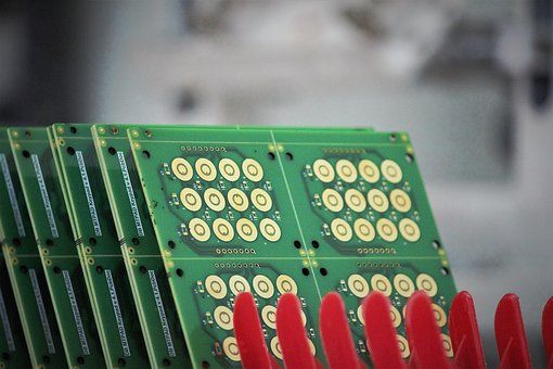
The process of designing a printed circuit board for aerospace and defense applications is complex and lengthy. It requires a high level of expertise and attention to detail to ensure that the board meets all of the necessary specifications and requirements.
The process begins with defining the circuit’s specific requirements. This includes determining the PCB components, their size and shape, and the necessary signal routing. After defining these requirements, the designer will begin the layout process.
During the layout process, the designer will place the components on the board, route the signal traces, and add any necessary layers or vias. It is critical that the layout is accurate and the circuit meets all of the requirements and performs well.
After the layout is complete, the board will undergo a series of tests to ensure that it is perfect in all ways. This includes testing for electrical performance, temperature range, and reliability. If there is any issue, the designer will have to redesign and retest the board.
You can build the board after thoroughly testing it. The manufacturer will follow the specifications provided by the designer and create a finished board that meets all of the necessary requirements.
Overall, the process of creating a custom circuit design for aerospace and defense applications is complex. It requires a high level of expertise and attention to detail. By working with an experienced circuit designer, organizations can ensure that their circuit designs meet the unique demands of these industries and perform reliably in even the most challenging environments.
Managing Radio Frequency
RF or radiofrequency is an important factor to consider while designing a PCB for military and aerospace. The RF components should be according to the required performance specs. The board should avoid EMI or electromagnetic interference to keep the nearby devices safe. Generally, the rigid PC Board is ideal for the aircraft cockpit, and instrumentation of the control tower.
Thermal Management
The designers should also consider thermal management while designing the circuit boards. It is hard to replace a faulty PCB when the satellite is in space as heat accumulation can damage the board. The best solution, in this case, is to use metal that can naturally dissipate heat, as cooling is not possible in the absence of air. Hence engineers use heavy copper of 4oz with 20 layers to dissipate heat. However, it makes it quite challenging to have good solder joints as heat goes away from the SMD points.
The Benefits of Working with an Experienced Circuit Designer
When it comes to designing circuits for aerospace and defense applications, experience is the key. Working with an experienced circuit designer can offer numerous benefits, including:
- Understanding of Unique Requirements: An experienced designer will have a deep understanding of the unique requirements and challenges of circuit design for aerospace and defense applications. This knowledge is critical in ensuring that the final product meets all necessary specifications and operates effectively in its intended environment.
- Attention to Detail: In aerospace and defense, precision and attention to detail are paramount. Experienced circuit designer has honed their skills over many years and knows how to design circuits that are both reliable and efficient. They should be able to spot potential issues before they become problematic, helping to minimize costly delays and rework.
- Access to Industry-Leading Tools: The designer should have access to the latest design tools and software, enabling them to create circuits optimized for performance, size, and cost. These tools can be expensive to obtain and use, making it difficult for those without experience to compete.
- Proven Track Record: the PCB designer should have a proven track record of success in designing circuits for aerospace and defense applications. This experience gives you the confidence that the final product will meet all necessary specifications and requirements.
- Collaborative Approach: Printed Circuit Board designer knows that collaboration is key to delivering a successful product. Experienced designers will work closely with your team to ensure to meet your project goals, and will keep you informed throughout the entire design process.
Final Thoughts
The aerospace and defense industries have unique demands when it comes to the design of printed circuit boards. Designers should have an understanding of the specific requirements of these industries to ensure that their PCBs meet the highest standards. The above information gives readers an insight into the challenges and considerations that come with design for the aerospace and defense sectors.
By adhering to industry standards, the design process for aerospace and defense circuits becomes more rigorous and meticulous. However, this level of attention to detail results in electronic systems that are more robust and reliable in even the harshest environments.
So, when it comes to circuit design for aerospace and defense applications, it’s essential to work with an experienced designer. They have the skills, tools, and knowledge necessary to create circuits that meet the unique requirements of these industries, ensuring that your product performs as expected. So, before starting your next circuit design project, consider partnering with an experienced designer to take your design to the next level.
Would like to know more about the Circuit design or PC Board assembly for Aerospace and Defense Applications? Email us at sales@pnconline.com