


Recent Posts
Category
What is a Gerber Viewer in PCB Design?

Gerber Viewer
A Gerber viewer is any software application that enables you to examine the contents of a Gerber file. While some of these applications need installation, others are available online and do not require downloading or installation. All you have to do to see your Gerber files online is upload them.
Gerber files
Before the establishment of Gerber files, there were no industry-standard guidelines for manufacturing printed circuit boards (PCB). The papers that included the Printed Circuit Board requirements contained a diverse range of information. There have been many instances of miscommunication and misunderstanding between consumers and manufacturing firms. Finally, universal interoperability across PCB designers and manufacturers has been achieved with the introduction of the Gerber format. In order to work with a file format independent of the CAE/CAD program being utilized, it allows the latter.
After the project has been finished and adequately monitored, it should be sent to the manufacturer. The designer may transmit securely, with prior permission with the business, any Gerber files generated by the export feature. Even though many applications automatically export to this kind of archive, all documents may be compressed in one zipped file. Many firms accept just one compressed file. Testing and checking your files with various Gerber viewers is usually intelligent practice before sending them to the producer. It is a great technique to be followed by all designers.
The Gerber format
These are vector documents consisting of a series of instructions that create a visual object flow. The directions for making the hole on the PC Board are also included. Nowadays, businesses that manufacture printed circuit boards need clients, nothing else. The essential program for electronic design contains and allows the export of the whole work to this format. It is thus the first thing an electrical designer should look for in his CAE program.

The standard format now used is RS-274X. It’s an extreme version in the same document as it contains:
• the draw and flash commands
• the XY coordinates
• the openings
• the configuration parameters
Versions of Gerber Files
Nobody needs to order a delayed printed circuit board (PCB). Ideally, you submit your design file to the PCB maker, and then the manufacturer organizes the manufacturing of the board based on your file and sends goods to you. However, the actual issue is not so easy. It typically takes such a long time since you submit your designed file to the final arrival of your board. Your discontent with your PC Board manufacturer will grow with increasing turn-time.
You may do a lot to reduce this time from your viewpoint throughout the whole process. After all, efficiency and efficiency are your responsibility. As connectors and translators for PCB engineers and PCB manufacturers, German files serve a crucial role in allowing manufacturers to understand design engineers’ thoughts and ideas. Excellent and dependable products may be produced successfully and efficiently. There are now three Gerber format versions available:
• Gerber X2 – the latest Gerber format, including stack data and characteristics
• RS-274-X – an extended Gerber format version and extensively used.
• RS-274-D – Gerber’s oldest version, progressively replacing RS-274-X.
Over the years, the Gerber file format has seen numerous modifications and upgrades. Thus Gerber files have been updated in many versions. The earliest version, also known as RS-274-D, is Standard Gerber. It is mainly out of usage today, and standard Gerber files are not acceptable on the official website of Gerber. Gerber is extended to include RS-274-X, commonly known as X-Gerber. Extended Gerber was introduced in 1998 and is a human-readable ASCII format. The previous format has been enhanced by incorporating information in graphics and pictures. Gerber’s latest version is Gerber-X2, an expansion of Gerber-X. It is compatible with most CAM programs and enables the user to add file characteristics.
These characteristics are like labels that offer picture file information and features. It also simplifies the transition of PCB designs from CAD to manufacturing. UCAMCO has just launched another version named Gerber X3. While not extensively utilized, UCAMCO believes that its interoperability with other applications and simplicity of installation will become the new norm.
Gerber Files Generation
PCB engineers should never be too indolent to create their Gerber files for the following two reasons. You cannot be sure that the PCB software you use is the same as the software used by your PCB Manufacturer. You must create Gerber files yourself if your PCB producer utilizes various PCB software, and additional discussion and validation will certainly cause extra time and delay the manufacturing process.
Although PCB manufacturer utilizes the same PCB design tools, it is still advisable to create Gerber files yourself since differences in software applications may also lead to potential mistakes. PCB design engineers should thus learn to create Gerber files themselves in order to guarantee delivery speed and reliability of end products.
Gerber files typically include driver layer, solder mask layer, and silkscreen layer design data. In addition, Gerber files should still be produced to prevent potential misunderstandings in two levels with the same design data. Distinct PCB design software has different Gerber file generating operation procedures.
Converting Gerber Files
Depending on the circuit design software you choose, you can generate Gerber files. There are many of these applications. However, some of them are popular with Proteus, Altium Designer, and CircuitMaker. Eagle is also one of the simplest to use. You will have to change your approach to various programs, but here are basic principles. Created by a firm called Gerber, Gerber’s format now includes standard PCB software that is generally recognized, capable of defining board imaging conditions, such as driver layers, solder mask layers, and legendary layers. The printed circuit boards are intended to produce additional board manufacture information based on which board production is started, using a specialist EDA system (Electronic Design Automation) or a CAD system (Computer-Aided Design).
PCB producers will not completely grasp all PCB design file specifics unless it includes the Gerber file as reference and guidance. For each picture of a circuit board, the Gerber format file is applied and may be used for both manufacture of bare boards and the assembly of PCB. For bare-board production, Gerber format is required by conventional photoplotters and other factories that want image data such as legendary printers, direct images or AOI devices, etc.
Simply stated, Gerber files format must be dependent from the beginning to the conclusion of the PCB manufacturing process. In connection with PC Board assembly, a stencil layer is included in the Gerber size, and component positions are controlled, which is also considered as important reference data for the assembly, assembly, and combinations of SMT (Surface Mount Technology).
You need to load your board to the design programme of your circuit. Sometimes this process is easy, but sometimes certain export parameters need to be adjusted. You must next utilize the CAM processor to convert your data to Gerber files. The duration of this procedure varies significantly depending on the size and complexity of the board.
Once you have completed your CAM processor, you will have a set of files labeled with the name of your board but various extensions. You must compress and submit your layer files, drawings, box guidelines, and inside layers to the PCB maker. In order to generate the required Excellon files, you must typically return to the CAM procedure.
Now that you have your Gerber file, maybe your question is how to convert a Gerber to PDF? You will need to locate an online service or application to convert Gerber files to PDF files. Many of these applications are online and do not need your computer to be downloaded or installed. Just upload and wait for the software to convert your files.
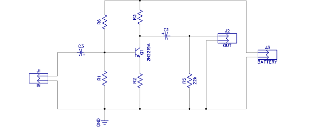
Example circuit diagram
The figure below, along with the 3D construction, illustrates the transistor amplifier wiring schematic. It is a promiscuous project, some of them in SMT with discreet components. The project contains elements, words, images, components, and more.
Final Thoughts
Gerber Viewer Software for Windows is a software program that allows you to read and examine Gerber files (GRB files) using its comprehensive toolkit. Some of these applications are also the software for the Gerber editor so that you may examine and modify Gerber PCB designs. The program may export the file viewer in different formats, such as SVG, PDF, PNG, PDF, JPEG, etc. If you wish, you may also print out the design.
PNCONLINE equipped with big and sophisticated machinery, are used CNCs may accomplish the more advanced versions are devoted to a particular operation or all jobs simultaneously. These machines start producing PCBs instantly without being linked to a computer and also can interpret Gerber client files directly thus equipped with processors. Other kinds of equipment, always in accordance with the Gerber requirements, can conduct circuit controls and automated optical inspections (AOI).
Interested in getting your PCB design done on an urgent basis in New Jersey? Get it done at PNCONLINE.
Contact us at sales@pnconline.com
Written by Sam Sangani

Sam Sangani is the President & CEO of PNC Inc., a Nutley, NJ based Printed Circuit Board manufacturer. Sam graduated from L. D. Engineering College with a BS Degree in Mechanical Engineering. He also continued his education and graduated from Steven’s Institute of Technology where he acquired a Master’s degree in Computer Science.
After completion of his BS, Sam worked as a QC Manager, for Xerox, Romania and London. He was responsible for the Quality Control of Cable and Wire Harness imports from Romania. After completing his Master’s Degree, he worked as a Senior Programmer with IBM, Tucson, Arizona. Sam was responsible for leading the Mainframe System Programming Team.
In 1997, Sam acquired PNC INC., a Nutley, NJ based PC Board fabrication Shop. From 1997-2013, Sam has made tremendous improvements and changes within PNC INC., as he added many new Products and Technologies in PNC’s portfolio. With his proven track record and leadership, PNC has never had an unprofitable year and has continued its growth yearly since 1997.
His current responsibilities are Strategic Planning, Corporate Management, New Business Ventures, Sales & Marketing, Trade Shows, Professional Services and leading productive teams to achieve peak potential. He has also utilized Lean Management techniques which have built a foundation for PNC’s high-paced growth. Sam also enjoys real-estate investing, web design & SEO, trading stocks, options, futures and Forex markets.


