


Recent Posts
Category
Printed Circuit Board thickness considerations and requirements
- Posted In:
- one stop pcb assembly
- pcb assembly
- pcb assembly and soldering
- pcb assembly contract manufacturer
- pcb assembly manufacturer
- pcb assembly near me
- pcb assembly services
- pcb assembly usa
- pcb board assembly
- pcb contract manufacturing
- PCB Fabrication
- pcb prototype assembly service
- printed circuit board assembly
- prototype pcb assembly
- turnkey pcb assembly
How Do You Select a Printed Circuit Board Thickness?
Selecting the correct PC Board thickness for your product requires balancing of three often competing aspects of the design: manufacturability, electrical performance and mechanical constraints. Modern PCB fabrication techniques at PNC give the PCB designer great flexibility in specifying the PCB lamination stack-up and gives them the option to design a PCB in a thickness other than the typical choices of .031”, 062” or .093”.
Manufacturing considerations in selecting a PCB thickness
To understand how to specify PCB thickness, it is important to understand how PCBs are fabricated. Most multilayer PCBS from 2 layers to 40 layers are constructed of these three basic materials.
- Core – a fully cured fiberglass panel usually with copper foil on both sides. It is essentially a two-sided Printed Circuit Board. PNC stocks cores in a variety of materials and thicknesses, down to 3 mils thick.
- Prepregs – fiberglass sheets impregnated with uncured epoxy resin. This resin will cure and harden when subjected to heat and pressure during the lamination process. It is the functional equivalent of double-sided tape. PNC also stocks prepregs in a variety of materials and thicknesses.
- Copper foil – used to create conductive layers. Copper foil thickness is chosen by the amount of current the traces in each layer of the board will need to carry.
Multilayer boards can be manufactured in a variety of thicknesses by mixing standard core thicknesses with standard prepreg thicknesses. The lower limit of PCB thickness is set by the number of layers and the minimum available core and prepreg thicknesses. Copper foil thickness also plays a small role in overall PC Board thickness.
Providing you want to stay with the standard thicknesses, I’ll give you an example of PNC’s standard core thicknesses based off the core copper thickness. Let’s take an .062 and compare the stack-ups. See Figure below:
Stack-up for an .062 multilayer:
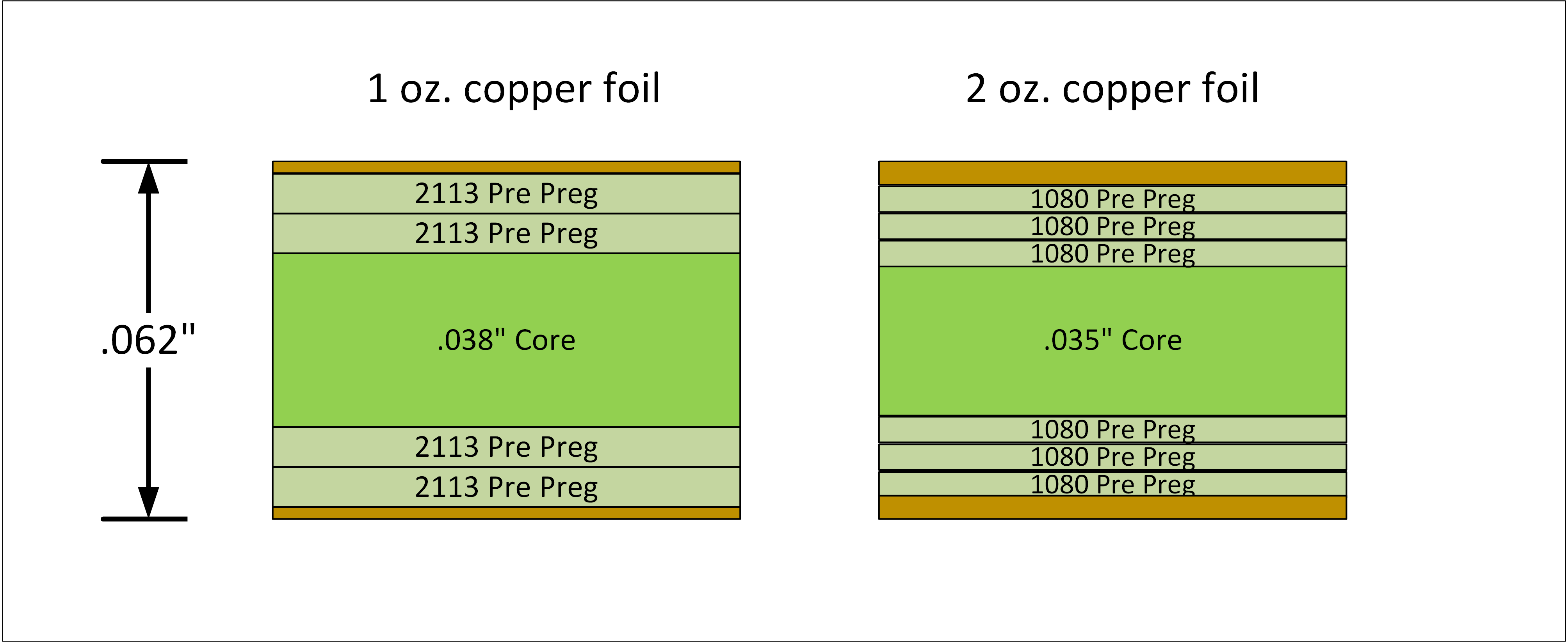
Notice to achieve the .062 overall thickness, the core thickness needs to be compensated based on the copper weight of the design. When using 1 oz copper we would use .038 core and .035 core for 2 oz. Also, the amount of pre preg would need to be adjusted as well to get to the thickness required. This is just one example when trying to determine overall thickness of your PCB.
The maximum PCB thickness is usually governed by something called the drill aspect ratio, which is the ratio of a drilled holes depth vs its diameter. When a hole is drilled, the deeper the holes becomes the harder it is to guide the drill accurately (because the drill deflects as it is pushed through the material) until you eventually reach a limit where you can no longer guarantee that the resulting drill hole will be centered in all the pads through the PCB. This is also referred to as drill wander in the PC Board fabrication world.
The aspect ratio for a through hole is the (board thickness) / (drill hole diameter).
Typically, the ratio is limited to approximately 10:1 This means that for a .062” thick board the smallest through-hole drill size is .006” which is the minimum drill size available at PNC. For a .093” thick PCB the smallest drill hole size will be .009” As board thickness increases, more complex via creation techniques such as laser drilled microvias are required to maintain the required pad density under components such as BGAs.
PCB thickness considerations for high speed circuits
One of the assumptions an electrical engineer makes when designing a circuit is that the PCB itself does not contribute any impedance to the circuit. However, in high-speed PCB design the integrity of the signals is definitely affected by the physical characteristics of the PCB.
Unfortunately for the designer the primary sources of parasitic capacitance and inductance of a PCB are affected by board thickness in conflicting ways, forcing the designer to carefully consider the trade-offs.
Vias
PCB vias can introduce both inductance and capacitance to the high-speed circuit. Parasitic inductance and capacitance of a via both increase proportional to board thickness.
Capacitance between layers
The capacitance between traces on different board layers or between traces and the ground plane are inversely proportional to the thickness of the dielectric between them. More space between layers will reduce parasitic capacitance and ensuring that all high-speed signal traces are the same distance from the ground plane will help impedance matching between them.
Crosstalk
Crosstalk between signal traces can be minimized by routing the PCB traces further apart and reducing the dielectric thickness between PCB trace and reference plane.
Mechanical Constraints
A PCB is ultimately a mechanical component of the product and is therefore subject to a variety of mechanical constraints. The PCB or PCBs must fit within the product envelope. This often requires that a PCB be as thin as possible. On the other hand, PCBs are subject to the torqueing forces from cables connected to the board edge and external connections. Preventing board failure during assembly or in use requires a circuit board fabrication thick enough to withstand these forces.
Finally, PCBs in the field are subjected to both vibration and shock. For example, large PCB panels can vibrate in several different modes when subjected to vehicle vibration, causing fatigue and eventual failure of solder joints. The rule of thumb is to get the resonance modes of a PCB to be 10X the input vibration. This requires designing thicker, stiffer PCBS and by careful placement and design of the PCB mounts.
These are the three most important considerations in selecting a PCB thickness. To optimize a PCB design, the PCB designer needs to understand all of these requirements and constrains on the PCB lamination stack-up, and have the flexibility to choose a PCB thickness that balances these often conflicting constraints. The team at PNC can help you design a PCB that meets your needs at a competitive cost and lead time.
Written by Sam Sangani

Sam Sangani is the President & CEO of PNC Inc., a Nutley, NJ based Printed Circuit Board manufacturer. Sam graduated from L. D. Engineering College with a BS Degree in Mechanical Engineering. He also continued his education and graduated from Steven’s Institute of Technology where he acquired a Master’s degree in Computer Science.
After completion of his BS, Sam worked as a QC Manager, for Xerox, Romania and London. He was responsible for the Quality Control of Cable and Wire Harness imports from Romania. After completing his Master’s Degree, he worked as a Senior Programmer with IBM, Tucson, Arizona. Sam was responsible for leading the Mainframe System Programming Team.
In 1997, Sam acquired PNC INC., a Nutley, NJ based PC Board fabrication Shop. From 1997-2013, Sam has made tremendous improvements and changes within PNC INC., as he added many new Products and Technologies in PNC’s portfolio. With his proven track record and leadership, PNC has never had an unprofitable year and has continued its growth yearly since 1997.
His current responsibilities are Strategic Planning, Corporate Management, New Business Ventures, Sales & Marketing, Trade Shows, Professional Services and leading productive teams to achieve peak potential. He has also utilized Lean Management techniques which have built a foundation for PNC’s high-paced growth. Sam also enjoys real-estate investing, web design & SEO, trading stocks, options, futures and Forex markets.


