


Recent Posts
Category
Motor Control EMI: AC Mains Conducted Emission
We do not want our product to come back from testing to find that we have failed electromagnetic interference (EMI) or conducted emissions (CE) exams. Furthermore, we do not want these noise sources to degrade our products performance, so we need to understand the mechanisms of this noise and how to minimize it.
One of the most common failures is, AC mains conducted emission testing which is listed as IEC 61326-1:2005, Ed. 1 section 7 (CiSPR11:2003). The purpose of the conducted emissions test is to measure noise currents that exit the products ac power cord to be sure the currents are within the regulated limits. The most efficient method for the reduction of conducted emissions is to reduce them at their sources. In this section we will discuss the source of conducted Emission on AC mains and how we can minimize the emissions. In following section we will focus on workarounds for the system has failed pass the AC mains conducted emission test.

Rectifiers:
Fast recovery diodes snap off sharply and generate high frequency noise compared to slow recovery diodes. In order to reduce this undesirable noise generated in the turnoff of the diode, snubber circuits are generally placed in parallel with the diodes. The snubber circuit consists of a resistor in series with a capacitor that acts as a path to discharge the charge stored at the diode junction when the diode turns off. This tends to smooth the diode current waveform, thereby reducing high frequency spectral content. The high frequency current will circulate through the snubber circuit where the leads need be kept short and the elements placed very close to the diode. In doing this, you will reduce the current loop area and the emissions will be radiated from the loop.
Transformer:
Winding the coils on top of each other introduces a parasitic capacitance between the primary and secondary. This primary-to-secondary capacitance can introduce an undesired coupling that allows noise on the secondary side to be more easily coupled to the primary side. Once the noise is present on primary side, it passes out through the power cord and is measured as a conducted emission by the LISN, unless the power supply is inserted between the power cord and transformer. The efficiency of this coupling, due to the parasitic primary-secondary capacitance increases at higher frequencies. In order to reduce this coupling, there is need for a metallic shield between the primary and secondary coils. This is referred to as a Faraday shield. This shield should be connected to the primary side reference or neutral.
Switching devices:
Primary current begins to flow when a MOSFET(s) is turned on. The transformer primary current ramping to a peak value is determined by input voltage, motor phase inductance, switching frequency and duty cycle. This trapezoidal (or triangular) current waveform is characterized in the frequency domain by a spectrum at the switching frequency. The harmonics are determined by the relative squareness of the waveform and causes the primarily differential mode emission currents to circulate between the AC mains and the power supply input. This current waveform can also create common mode emissions, due to radiated magnetic fields when the current path defined on the PC board layout encircles a large physical area.
The spectral content of the noise that is produced by switching is directly dependent on the rise and fall times of pulses. The slow (high) rise and fall times are desirable from the standpoint of EMC. This causes the MOSFET to spend more time in its active region, which increases its power dissipation, therefore is an undesirable result from the standpoint of thermal consideration. Concurrently, there is an apparent tradeoff between reduction of noise spectral content that will contribute to conducted emissions and the thermal heating of the switching element and related efficiency of the switcher.
Wire Harness and System connections:
Noise current sources appear between live and neutral connections without reference to the earth connection. In circuits with a switching power supply or motor control, the RF emissions are dominated by interference developed across the DC link to the switching devices. Although there will be a bulk capacitor, the high di/dt through this capacitor will generate voltages at the harmonics of the switching frequency across its equivalent series impedance.
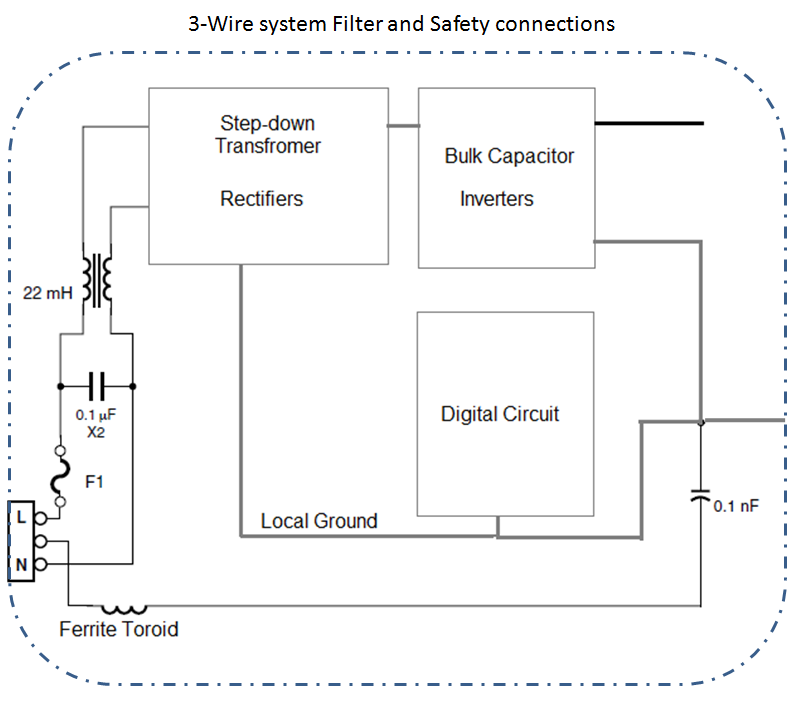
The coupling is dominated by the inter-winding capacitance of the isolating transformer, stator-rotor of the motor and system to the chassis. These capacitances are referred to earth, either directly or via the enclosure if this is conductive. A well shielded enclosure will minimize “leakage” of this capacitive coupling and hence reduced conducted emissions. Ideal connections for 2-wire and 3-wire system are shown in figure xx and xx.
<br\>
This article was written by Sam Sangani Jr., PNC Inc.’s Fellow Design Engineer. For additional information related to this or any other topic, you can reach Sam via e-mail at sam@pnconline.com.
Written by Sam Sangani

Sam Sangani is the President & CEO of PNC Inc., a Nutley, NJ based Printed Circuit Board manufacturer. Sam graduated from L. D. Engineering College with a BS Degree in Mechanical Engineering. He also continued his education and graduated from Steven’s Institute of Technology where he acquired a Master’s degree in Computer Science.
After completion of his BS, Sam worked as a QC Manager, for Xerox, Romania and London. He was responsible for the Quality Control of Cable and Wire Harness imports from Romania. After completing his Master’s Degree, he worked as a Senior Programmer with IBM, Tucson, Arizona. Sam was responsible for leading the Mainframe System Programming Team.
In 1997, Sam acquired PNC INC., a Nutley, NJ based PC Board fabrication Shop. From 1997-2013, Sam has made tremendous improvements and changes within PNC INC., as he added many new Products and Technologies in PNC’s portfolio. With his proven track record and leadership, PNC has never had an unprofitable year and has continued its growth yearly since 1997.
His current responsibilities are Strategic Planning, Corporate Management, New Business Ventures, Sales & Marketing, Trade Shows, Professional Services and leading productive teams to achieve peak potential. He has also utilized Lean Management techniques which have built a foundation for PNC’s high-paced growth. Sam also enjoys real-estate investing, web design & SEO, trading stocks, options, futures and Forex markets.


