


Recent Posts
Category
Improving Speed by PCB Routing Techniques in PCB Layout

There has been immense development in physical design aspects of designing with the advent of CAD Tools. It’s not that long ago, that we were hand taping on multiple layers of mylar at 2:1, 4:1 and even 8:1, and then having to shoot the artwork with a camera to reduce the film to 1:1. The power of today’s CAD tools can maximize your time whether it be circuit design, circuit simulation, PCB design, or system-level simulation of PCB Layout. In turn, Complex designs can be optimized quicker and more efficiently.
We know that copper traces are used as interconnects or bridges between two unconnected elements of the circuit. The length & shape of these interconnects play an important role in high speed design, since each interconnect is modeled as a combination of resistance, inductance and capacitance, which can in turn change the value of impedance. Taking this into consideration, we try to model PCB Routing Techniques in a more algorithmic and efficient way to improve the speed of the design.
The most challenging task for the designer is the placement of the components in order to minimize the usage of wire and chip area. The design starts with placing the important components of the circuit in terms of design and the entire board to reduce the routing constraints. Finalizing the key elements specific locations (critical components) and routing paths helps in analyzing the critical path and operating frequency of the circuit design. After Placement, particularly for routing a wide variety of analog and digital signals, with varying voltages and currents, ranging from dc to high frequency (GHz), the utmost importance is keeping signals from interfering with one another. The Zero potential planes help in providing a common reference point for devices as well as helping device shielding in order to compensate for any extra amount of current. In the case where signal isolation is required, we need to concentrate on the physical distance between the signal traces.
Major Routing key points
- Distance between two interconnects must be minimized for particular path.
- There should be no sharp bends, (90 Deg.) in the track design.
- Tracks should exit from the center of a connection point, avoiding other interconnects and pads in order to have a high speed and error free design.
- Do not place via under component.
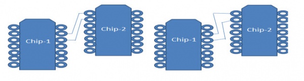
Image: Proper angle routing (left) and bad routing (right)
Reduction in long traces on adjacent layers to prevent capacitive coupling.
- Reduction in long parallel runs and close proximity of signal traces in order to reduce or eliminate inductive coupling (practically impossible) in a design.
- Signal traces requiring high isolation should be routed on separate layers and if not possible, orthogonal routing can be done. Orthogonal routing will help in minimizing the capacitive coupling which will lead to the shielding effect by the ground or zero potential.
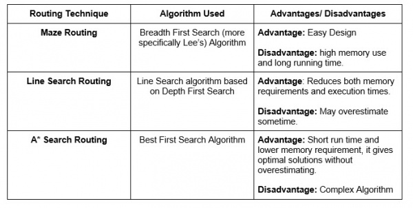
Automated Routing Techniques can be used for increasing speed
Auto routing within a Design exhausts all the possible implementations of the given possible design and helps to improve the performance, reliability and cost of the circuit design. This innovation is referred to as Electronic Design Automation. The technology has advanced with usage of Artificial intelligence and neural based technology. Automated routers are mainly used when you have a complex board with little routing space. Advanced automated routers allow you to specify exactly how you electrically want to layout the most important tracks. Below is the list of general purpose routing techniques and algorithms (These are algorithm models related to CAD Routing tools) , apart from this there are special routing techniques for power and clock like H-clock tree synthesis.
Example of High Speed PCB Routing Technique
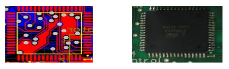
Top Layer PCB Design and Final Chip Implementation
The left hand side of the above diagram shows the top view implementation of a PCB design. Due to the simplicity of this design, we can mount all the circuit components on the top layer. The above design will help in eliminating the signal trace which ensures the best possible speed and design of the circuit. The key points in this PCB design is the reduced delay time because the separation of larger bypass caps are placed farther away with ferrite Chips for HF isolation of currents and multiple via which reduces the delay path in the circuit.

Written by Sam Sangani

Sam Sangani is the President & CEO of PNC Inc., a Nutley, NJ based Printed Circuit Board manufacturer. Sam graduated from L. D. Engineering College with a BS Degree in Mechanical Engineering. He also continued his education and graduated from Steven’s Institute of Technology where he acquired a Master’s degree in Computer Science.
After completion of his BS, Sam worked as a QC Manager, for Xerox, Romania and London. He was responsible for the Quality Control of Cable and Wire Harness imports from Romania. After completing his Master’s Degree, he worked as a Senior Programmer with IBM, Tucson, Arizona. Sam was responsible for leading the Mainframe System Programming Team.
In 1997, Sam acquired PNC INC., a Nutley, NJ based PC Board fabrication Shop. From 1997-2013, Sam has made tremendous improvements and changes within PNC INC., as he added many new Products and Technologies in PNC’s portfolio. With his proven track record and leadership, PNC has never had an unprofitable year and has continued its growth yearly since 1997.
His current responsibilities are Strategic Planning, Corporate Management, New Business Ventures, Sales & Marketing, Trade Shows, Professional Services and leading productive teams to achieve peak potential. He has also utilized Lean Management techniques which have built a foundation for PNC’s high-paced growth. Sam also enjoys real-estate investing, web design & SEO, trading stocks, options, futures and Forex markets.


