


Recent Posts
Category
HOW DOES SMT ASSEMBLY WORK?
While modern designs for electronics get smaller, more designers depend on the technique of surface mounting. After the 80’s, this technique became famous and hasn’t stopped being the dominant PCB assembly technology for electronics production.
Almost all of the devices in your pocket – either an iPhone xs max or a smartphone – has probably been produced using surface mount technology (SMT). Most of those components in your vehicle or Transportation today have probably been assembled using SMT.
What is Surface Mount Technology (SMT)?
Assembling electronics with SMT involves assembling electrical parts using automated equipment that places components on the printed circuit board (PCB).
Manufacturing devices using surface mount technology (SMT) essentially imply electronics assembly using machine tools. In contrast to traditional THT procedures, SMT elements are put directly on top of the PCB rather than soldered to a radial or axial lead. SMT has been the most commonly utilized method in the business when it comes to ethernet interfaces.
Placement and Assembly of Components:
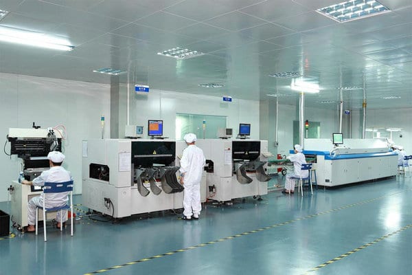
The components to be assembled are inserted into the pick and place feeders or trays. Intelligent software applications guarantee that components are not unintentionally swapped or misloaded during the config file. The SMT pick and place machine then autonomously takes each part from its tray or reel using a pressure pipette and puts it in its proper location on the panel using accurate X-Y cross pre-programming. Our equipment can assemble up to 24,000 parts per hour. Just after SMT assembling has been finished, the PCBs are transported to soldering reflow ovens.
Soldering Components:
The reflow-soldering technique is utilized for series manufacturing orders. This method involves placing PCBs in a nitrogen assisted environment. It is then progressively heated with hot air when the solder paste melts, and the flux vaporizes and attaches the parts to a PC Board. The panels are cooled down after this step.
Solder Paste Usage:
A few of the initial stages in SMT manufacturing is the administration of the solder paste. Solder paste is squeeged through aperature openings in a stainless steel stencil. Once the squeegee passes over the stencil, the PCB is lowered and travels to the next operation, solder paste inspection, known as SPI. After the solder paste has been verified, the PCB’s move to the SMT pick and place machine.
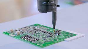
AOI System in SMT:
AOI visual inspections should be carried out for virtually all manufacturing orders in verifying the quality of completed panels or to capture and rectify an error. The AOI section analyzes each Printed circuit board with multiple cameras and analyzes the look of each circuit to the proper, pre-defined sample image. They will either fix the error or remove the panel from the device to examine it further. The AOI visual management guarantees consistency and precision in the manufacturing process of the SMT assembly.
SMT Components that are not Suitable for Auto Pick & Place:
While most components are placed automatically, others are not installed. This can be for several reasons. Some of them are,
Ø Thermal stress:
Other circuits may be too resistant to thermal and are not perfect materials for soldering reflow temps. These materials must be installed manually to protect them following the usual assembly procedure.
Ø Too light:
Specific components are not substantial enough and, consequently, have a low bulk ratio for conventional soldering automated placing equipment.
Ø Rugged solder joints:
Many components, like connection leads, require a stronger solder joint. Some components are soldered manually to enable this.
This enables rapid examination and repair of components that may be at risk of layout for infringements before the soldering oven is passed.
Surface mount technology benefits:
As with cross-holes, both advantages and drawbacks are included with SMT. Let’s start with some SMT design advantages:
1. Efficiency:
Thanks to SMT technology, designers can now transform complicated circuits into smaller PCB’s.
In contrast with using the storage on a PCB more efficiently, the SMT board is quicker to increase its overall capacity.
2. Fewer mistakes:
SMT assembly is very reliant on technology and not so very dependent on people. SMT is a far less error-prone procedure since it’s nearly fully automated.
3. Cost Accessibility:
These are some of the reasons for the SMT module was to reduce cost. SMT needs far fewer holes in the circuitry. This substantially reduces manufacturing and handling expenses. Furthermore, SMT is much more able to produce large quantities, thereby improving the unit cost.
SMT Disadvantages:
As with other production processes, SMT design has certain drawbacks. The most important is that it needs considerably more eye for detail than a complete construction. Even if the process is substantially automated, your specifications must still be fulfilled to create quality. This is mainly the responsibility of the inventor and the producer of the electronics equipment.
There may also be problems when SMT can be used to put parts on a PCB that works under circumstances that include:
- Machine stress
- Ecological stress
- Stress of temperature
This issue may be addressed by mixing SMT with complete processes to achieve both advantages. That’s correct — on the very same pitch, you may utilize both!
What is the SMT-SMD Difference?
The distinction between SMD & SMT is that SMD relates to the electronic element placed on a Board. SMD is an integrated circuit.
Surface mount technology (SMT) refers in contrast to the way electrical components are placed on a printed circuit board.
SMT refers to Surface Mount Technology and is the complete technology used to place and solder electronic parts on printed circuit boards or PCBs such as resistors, condensers, transistors, electronic components. The devices utilized are also known as surface mounting devices (SMD), surface-mount devices. It should be pointed out that SMT does not have to preserve for constituent pins utilizing holes, and SMD is considerably smaller than by-pass technology.
SMT features:
- Parts do not have connections or short leads alone;
- On the same edge of the PCB, the top part of the device and the solder joint;
SMD features:
- miniaturization;
- No plumage (flat / short plumage);
- authoritative Parenting for PCB assembly mounting;
Uses of Surface Mount Technology:
SMT mounting was developed to produce a better, more robust electrical product.
Many typical uses for surface mounting technology are shown if you look around your workplace or home area. Anytime you need a commodity, turn to the surface mount Device structure:
- Shorter
- Thinner
- Faster
- Most potent
While an SMT assembly is still utilized in some situations or even in specific places aboard.
Summary:
Utilizing the surface mounting technique for electronic engineering, electronic modules are integrated using automated machines which put various elements onto a PCB.
Contrary to typical technological procedures, SMT components are put directly on the surface of the printed circuit board rather than soldering to a lead. Although an SMT device may seem quite complex, it operates extremely fast. The base of the SMT machine utilizes a tiny vacuum head to collect the parts before putting them accurately in the circuit. These devices, known as “pick” and “place” devices, pick up bits from a periodical and position them on a vacuous circuit board. It is important to remember that the correct programming of these devices plays a significant role in efficiency and durability.
Written by Sam Sangani

Sam Sangani is the President & CEO of PNC Inc., a Nutley, NJ based Printed Circuit Board manufacturer. Sam graduated from L. D. Engineering College with a BS Degree in Mechanical Engineering. He also continued his education and graduated from Steven’s Institute of Technology where he acquired a Master’s degree in Computer Science.
After completion of his BS, Sam worked as a QC Manager, for Xerox, Romania and London. He was responsible for the Quality Control of Cable and Wire Harness imports from Romania. After completing his Master’s Degree, he worked as a Senior Programmer with IBM, Tucson, Arizona. Sam was responsible for leading the Mainframe System Programming Team.
In 1997, Sam acquired PNC INC., a Nutley, NJ based PC Board fabrication Shop. From 1997-2013, Sam has made tremendous improvements and changes within PNC INC., as he added many new Products and Technologies in PNC’s portfolio. With his proven track record and leadership, PNC has never had an unprofitable year and has continued its growth yearly since 1997.
His current responsibilities are Strategic Planning, Corporate Management, New Business Ventures, Sales & Marketing, Trade Shows, Professional Services and leading productive teams to achieve peak potential. He has also utilized Lean Management techniques which have built a foundation for PNC’s high-paced growth. Sam also enjoys real-estate investing, web design & SEO, trading stocks, options, futures and Forex markets.


