


Recent Posts
Category
Grounding in Printed Circuit Board Design

As we advance into the future, we want everything to be faster, cheaper, compact and durable. Everything around us is electrical. Moore’s law predicted that numbers of transistors per square inch of Printed Circuit Board will double every 2 years and it’s been true too date. Well theoretically it sounds good. But implementing new products with the above requirement comes with a cost. In order to reduce the unit cost of the design, due to noise. Various techniques have been developed in the past few decades to reduce noise in the circuits as the number of components increases and the available size decreases. Design techniques include proper grounding, decoupling, routing and signal multiplexing.
Grounding at PCB level can be in implemented as single point ground. As the name suggests a single point ground is where the complete circuit residing on the PCB has a single ground. This technique is developed by using a ground plane. Ground plane is defined as a highly conductive electrical surface which will be used as a system ground. In printed circuit boards, it is referred to as a large conducting surface of copper foil on either side of the PCB. It is connected to the power supply ground terminal and thus it serves as a return path for current from different components on the board .The fact that a large surface area of highly conductive metal, like copper, has a very low impedance which forms the basis of this method.
Ground plane is laid on the PCB, such that it covers the maximum area which is not occupied by circuitry itself. In multilayer PCB’s, it is often a separate layer covering the entire board. This makes the circuit design easy to implement, thus further allowing the designer to ground any component or subpart of a circuit without adding additional traces. The large area of copper which provides a very low impedance path conducts the large currents originating from other components/subparts without significant voltage drops. This ensures that the ground connection of all the components is at the same reference potential.

Benefits of grounding in PCB are:
- Reducing electrical noise
- Reduce interference being coupled from one part of the circuit to another.
- Reducing crosstalk between adjacent circuit traces.
1) Noise reduction:
When circuits switch states, large current flows from the active devices through the ground. If the power supply and ground traces have noticeable impedance, then the voltage drop across them may create noise voltage that would disturb other parts of the circuit. The large conducting area of the ground plane has much lower impedance than a circuit trace, so the current causes less disturbance.
2) Interference & Crosstalk reduction:
When two traces are placed too close to each other, an electrical signal in one can be coupled into the other. This is due to electromagnetic induction caused by the linking of magnetic field lines from one trace to other. This phenomenon is known as crosstalk. When a ground plane layer is present underneath the circuit in the PCB, it acts as a transmission line for the trace. Thus the direction of current flowing through the ground plane is opposite to the direction of current flowing through the circuit trace. This cancels most of the electromagnetic fields and consequently reduces crosstalk.
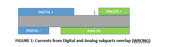
Many of the present day circuits consist of both Analog and Digital subparts. To avoid current from one subpart to affect the other subpart, ground planes are split and then connected by a thin trace. The thin trace has low enough impedance to keep the two sides very close to the same potential while keeping the ground currents of one side from coupling into the other side, completing a ground loop.

Thus grounding in PCB can significantly improve the circuit/chip performance. No extra area is added to the chip as leftover areas are used. This method doesn’t add too much of cost to the initial design which makes it readily acceptable at industry level.
Types of single ground connection:
-
- Series Ground Connection:
-
- Parallel Ground Connection


Written by Sam Sangani

Sam Sangani is the President & CEO of PNC Inc., a Nutley, NJ based Printed Circuit Board manufacturer. Sam graduated from L. D. Engineering College with a BS Degree in Mechanical Engineering. He also continued his education and graduated from Steven’s Institute of Technology where he acquired a Master’s degree in Computer Science.
After completion of his BS, Sam worked as a QC Manager, for Xerox, Romania and London. He was responsible for the Quality Control of Cable and Wire Harness imports from Romania. After completing his Master’s Degree, he worked as a Senior Programmer with IBM, Tucson, Arizona. Sam was responsible for leading the Mainframe System Programming Team.
In 1997, Sam acquired PNC INC., a Nutley, NJ based PC Board fabrication Shop. From 1997-2013, Sam has made tremendous improvements and changes within PNC INC., as he added many new Products and Technologies in PNC’s portfolio. With his proven track record and leadership, PNC has never had an unprofitable year and has continued its growth yearly since 1997.
His current responsibilities are Strategic Planning, Corporate Management, New Business Ventures, Sales & Marketing, Trade Shows, Professional Services and leading productive teams to achieve peak potential. He has also utilized Lean Management techniques which have built a foundation for PNC’s high-paced growth. Sam also enjoys real-estate investing, web design & SEO, trading stocks, options, futures and Forex markets.


