


Recent Posts
Category
Basics of Solder Paste selection for PCB Assembly
INTRODUCTION
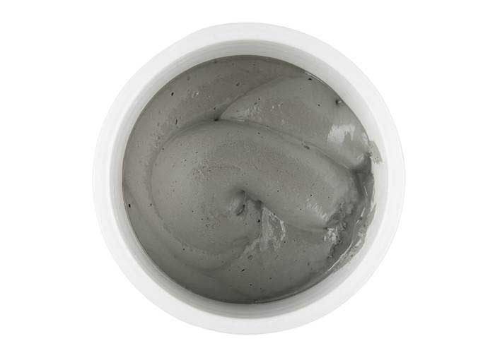
Solder pastes are amorphous putty-like soldering materials used to solder surface-mounted components to the Printed Circuit Board. The effect of solder paste on the PCB’s structural and functional integrity is the paramount factor to consider when deciding on selection of solder paste for application. Many factors which contribute towards the strength of the solder joint and its conduction efficiency need to be addressed as well. This is not just a discussion on what measures and precautions to take during PCB assembly and reflow, but also to put into question what a PCB design engineer should consider when designing a PCB and how the layout should adapt to the corresponding solder paste properties to yield the best result. It is a very brief introduction towards an expansive topic like solder pastes which will be discussed in further detail in future posts.
PROBLEM STATEMENT
A big concern for manufacturers arises when they need to select the right solder paste for SMT applications that is best suited to the PCB assembly and the manufacturing setup. A regular PCB has different types of components, all of which cannot always be compatible with the one solder paste applied across the board and thus, need some necessary compromises in solder selection. PCB designers should be educated about solder paste application and properties in SMT manufacturing to increase reliability of product yield.
SOLDER PASTE BASICS
Solder pastes are categorized based on the following characteristics: RoHS compliance (solder composition), flux type, grain size etc. RoHS (Restriction of Hazardous Substances) is a directive which mandates the exclusion of lead and other hazardous materials from solder pastes and manufacturing processes and aims to reduce environmental and occupational hazards related to electronics manufacturing. It has been adopted as a standard for commercial applications while only military applications can use leaded manufacturing processes. Many components now specifically require RoHS or non-RoHS procedures for PCB Assembly.
Flux is a chemical resin that is used to facilitate the soldering process. It is responsible for removing dirt and preventing oxidation of the component tips during reflow. They can be classified as either water-soluble fluxes or no-clean fluxes. Water soluble fluxes can be cleaned by using water while no-clean fluxes produced low levels of residue which are not necessary to clean but it is advised to clean with designated chemical wash to provide better result.
Solder pastes consist of solder grains which are available in different sizes which are given numerical designations from Type 1 to Type 8 based on descending order of solder grain sizes. Decrease in solder grain size also highlights the advancements in solder technology where Type 1 was adopted first, and Type 8 is the latest addition to minimum achievable solder grain size.
SOLDER PASTE
Since 2006, commercial solder pastes were manufactured and used without lead and other hazardous materials like cadmium and mercury in accordance with the RoHS directive. The directive also affected key PCB fabrication processes and successfully eliminated usage of hazardous materials for commercial applications. Lead in a traditional tin-lead alloy solder is responsible for lowering the melting temperature of the solder to approx. 183°C and it also helps slow down the rate of tin whisker growth in electronics. The process of finding replacements to maintain those advantages offered by lead is still ongoing. Lead-free solders have higher melting points and are more expensive than leaded solders.
The most popular lead-free solder currently being offered is tin-silver-copper alloy which has a melting temperature of approx. 217°C. This has also resulted in components like resistors, transistors being conformed to RoHS compliance. The main drawback of maintaining RoHS compliance for the product is that it is significantly more expensive than leaded processes and does not yield any benefits of switching to lead-free options. The effect of RoHS directive on component manufacturing and the larger effect on electronics manufacturing will be discussed in detail in future posts.
As of today, Type 3 solder is the most widely used solder paste. The following comparison consists of certain superficial characteristics which are a good point to start at before diving into a thorough discussion for each and exploring more complex properties and features of solder pastes. The reason behind comparing T3, T4 and T5 specifically is that T4 and T5 were recently adopted for mass usage for finer and smaller footprints in the PCB assembly industry while T3 has been the industry standard for a long time.

It is important to note that the sensitivity and reactivity of solder paste to temperature change increases as the solder grain size decreases. This is due to increase in the number of solder grains occupying the same area as the solder grain size decreases. Simply put, the greater the number of solder particles in a given area, the more reactive that particular area of solder will be. Therefore, from this we can conclude that T4 solder will melt at a lower temperature than T3, and T5 will melt at a lower temperature than T4. The advantages, disadvantages and the various effects of using small grain-size solders on component structure and performance will be discussed in further detail in the next post.
FLUX
Fluxes are infused in the solder paste and they are released during reflow. The flux is always released before the solder can melt to provide an oxidation-free environment. Its chemical profile consists of a natural or synthetic resin to coat the component pins and pads, activators to release the flux at the right temperature, solvents to facilitate deposition of solder on the joint, and additives to compensate for any modifications in flux composition. Water-soluble and no-clean fluxes are both used in various situations based on the amount of oxidation occurring during reflow, the level of reactivity of the solder, solder grain size, material of the board, and surface finish of the board.
No-clean fluxes are generally used for boards where the corrosion resistance of the surface is weak. It yields low residue on the printed circuit board assembly because the flux either burns off during reflow or it forms noncorrosive, localized residue around the solder joints. Contrary to its name, it does require cleaning post-reflow but less so than most other high-residue fluxes. No-clean solder pastes are used as an industry standard by most electronics manufacturing service providers because of its ease of use. The main drawback of using no-clean flux is that since it is less corrosive, it does not provide as much protection from oxidation as water-soluble flux but that has to be accepted as a trade-off for better quantitative results in large-scale production.
Water-soluble fluxes are generally used for precise action and give excellent results but the main drawback is that they require careful application and condition regulation due to their highly reactive and corrosive nature, and the difficulty in cleaning them post-reflow. Compared to no-clean flux, it produces more residue that cannot be removed easily from the board and due its high corrosivity, it may damage the PCB surface and component leads. Cleaning unwanted residue off the board requires additional machinery which occupies valuable space on the shopfloor. This limits its usage in the industry to only customer requests or specifications to use water-soluble solder pastes.
KEY CONSIDERATIONS FOR PCB DESIGNING
It is important to consider how solder selection will affect your PCB design. For simplicity, the effects will be divided based on solder paste composition, solder size and flux usage. Many of these considerations may overlap or may have to be used in conjunction for achieving the best result.
SOLDER PASTE COMPOSITION:
• Components used on PCB should be first checked to see if they are RoHS compliant or not, based on the solder paste used. Components with RoHS compliance usually have different leads which may or may not be compatible with leaded solders, and it may affect the solderability of the component to the copper pads, the solder joint’s mechanical strength, and component shelf-life and performance. It is also important to ensure the components operating and manufacturing parameters meet the solder paste properties, otherwise components may get burned or dysfunctional during the reflow process, leading to visible or latent component failure.
• Flux selection should be based on solder paste composition. Flux release at specific temperatures should be done in conjunction with the reflow profile for that specific solder paste. Solder melting and flux activation occur at different instances in the reflow process. Early activation of flux may cause surface corrosion, component failure, early burn-off which may lead to poor soldering and late activation may lead to increased oxidation during reflow process along with difficulty in cleaning.
SOLDER SIZE
• Solder grain size should also be considered when choosing component package and its corresponding design footprint on the Printed Circuit Board. Larger footprints do not require smaller grain-size solders. If the grain size is small, say T5, then based on its high reactivity, more number of particles per unit area and greater wetting ability, solder may flow too easily on melting resulting in solder defects which will affect component performance and product life-cycle. The reverse situation, where small footprints are used in conjunction with large grain-size solders, also leads to solder defects.
• Component package selection will also affect stencil aperture size, stencil thickness and solder deposition efficiency. Using large-size solders, say T3 solder, for micro-BGA or 01005-imperial sizes will result in gasketing and insufficient paste deposition; while using small-size solders, say T5 solder, for large footprints may result in bridging.
• The spacing between footprints of separate components, spacing between component leads of the footprint on the Printed Circuit Board should change based on the solder grain-size as using large grain sizes for small footprints, and vice versa, will lead to solder bridging which will in turn affect device performance and life-cycle.
FLUX COMPOSITION
• PCB thickness, material and coatings should be selected based on flux used for the reflow process. One should avoid using water-soluble fluxes for a thin PCB as they are highly corrosive in nature and may lead to excess surface corrosion. Corrosion resistant material and coatings should be used in accordance with the flux selected, as not using them will lead to corrosion and cleaning issues and using them when not needed(say a no-clean flux is being used) will increase cost of production.
All PCB’s should be designed keeping in mind the effects of solder paste, stencil design, flux, process used on
SMT assembly PCB’s. Some of these topics and more will be added to the list and discussed in further detail in the future.
Written by Sam Sangani

Sam Sangani is the President & CEO of PNC Inc., a Nutley, NJ based Printed Circuit Board manufacturer. Sam graduated from L. D. Engineering College with a BS Degree in Mechanical Engineering. He also continued his education and graduated from Steven’s Institute of Technology where he acquired a Master’s degree in Computer Science.
After completion of his BS, Sam worked as a QC Manager, for Xerox, Romania and London. He was responsible for the Quality Control of Cable and Wire Harness imports from Romania. After completing his Master’s Degree, he worked as a Senior Programmer with IBM, Tucson, Arizona. Sam was responsible for leading the Mainframe System Programming Team.
In 1997, Sam acquired PNC INC., a Nutley, NJ based PC Board fabrication Shop. From 1997-2013, Sam has made tremendous improvements and changes within PNC INC., as he added many new Products and Technologies in PNC’s portfolio. With his proven track record and leadership, PNC has never had an unprofitable year and has continued its growth yearly since 1997.
His current responsibilities are Strategic Planning, Corporate Management, New Business Ventures, Sales & Marketing, Trade Shows, Professional Services and leading productive teams to achieve peak potential. He has also utilized Lean Management techniques which have built a foundation for PNC’s high-paced growth. Sam also enjoys real-estate investing, web design & SEO, trading stocks, options, futures and Forex markets.


