Tag Archives: pc board assembly

What is High TG In PC Board Fabrication?

The making of PCB involves different steps, technologies, and terms, and TG is one such term that refers to the Glass Transition Temperature. High TG PCB is the board made at a high temperature. We will discuss this topic in detail, including the TG value, features, applications, materials, parameters, and much more.

What is High TG PCB?

If a PCB’s temperature goes beyond a set TG value, its condition will change. Like, the solid board will turn rubbery, affecting a PCB’s function. Depending on where you use a PCB, the temperature of the application should be at least 10 to 20C less than the PCB temperature.

Understanding TG Value

TG means Glass Transition Temperature like there is a certain limit of this temperature for PCB and that specific temperature is the TG value. TG value helps in understanding the PCB material, and you can find which temperature is required for its service.

Secondly, it helps you to find the condition of the PCB material, like if it’s solid, flexible, or solid-flex.

High TG PCB and Its Features

You have to choose a high TG Printed Circuit Board for your application carefully, because it involves multiple features, including thermal, electrical, mechanical, and chemical features.

Thermal Features: they include the TG or Glass Transition Temperature, thermal conductivity, thermal temperature’s coefficient, and decomposition temperature. TG is the temperature at which the state of the PCB material changes. But, when the board cools down, it gets back to its initial condition.

Electrical Features: they include the surface resistance, electrical power, volume relativity, and the dielectric constant and loss tangent.

Chemical Features: the chemical properties of a high TG PCB include the moisture absorption and the methylene chloride resistance of the PCB material. The TG PCB should be able to resist moisture if it’s near water.
Mechanical Features: the mechanical features are also important to know regarding the TG PCB. They include the flexural and peel strength, and the young’s module.

Suitable Materials for High TG PCB

A PCB has two materials, including laminate and substrate. The substrate includes epoxy resin, glass, or paper weave. The substrate should be compatible with the TG. Some common substrates that we use for a high TG PCB are;

  • CEM-1, 2, 3,4, and CEM-5
  • G-10 and 11, FR-1 to FR-6
  • Aluminum
  • Knapton
  • Pyralux

The last three materials are flexible.

The laminates should also be compatible with your TG PCB in terms of strength and temperature. Some common laminates are:

  • FR-1, and FR-4
  • CEM-1, CCEM-3
  • Teflon

Criteria for High TG PCBs

Printed circuit boards with a high TG value are based on certain criteria as described below:

  • The selection of a PCB, depending on the components like it can be single or double-sided PCB or embedded.
  • The stack-up PCB with a single layer or several layers
  • The design of such boards can be based on a module or it can be custom
  • The strength of the board also matters, like it should be robust either electrically or mechanically
  • PCB’s bendability also helps to classify the TG PCB, like if it’s hard, flexible, or hard-flexible
  • The electrical strength also helps classify the TG PC Board

Generally, manufacturers use bendability and strength to classify a TG PCB‘s physical properties.

Where Can You Use The High TG PCBs?

You can use the high TG circuit boards in intense conditions, as the environments with high-vibration devices. They are also suitable for applications with shocks, chemical components, and high temperatures. Like, missiles and car parts often come up with chemicals. So, the suitable industries for high TG PCBs include aerospace, telecommunications, military and defense force, automobile, and down-hole drilling.

What to Consider While Designing a Rigid PCB?

You must hire a professional PCB manufacturer for the right design, manufacturing, and assembly of these boards. The engineer must know the kind of environment that suits a TG PCB to function precisely. Below are a few examples to help you understand it.

Commercial Use

Many telecommunication companies use the best materials for mobile devices to enable them to bear high shocks. Like, the phone should not get damaged easily when you drop it.

Auto Industry

PCB has to be safe under a car’s hood as it’s mostly vibrating, so a shock or crash might happen. Hence, a rigid PCB is the best solution in this case.

Aerospace Industry

The flying machinery always needs the high TG PCB because there is intense vibration, like in the jet engine, as there are thousands and millions of micro-vibrations in one minute. So, equipment related to aerospace should be able to tolerate extreme temperatures, like from -45°C to 85°C.

Other Applications

These boards are also ideal for solar power equipment, such as power inverters and cogeneration equipment. As these boards resist temperature, they work well in many industries. Like, one of its applications involves Lead technology, like the medical, computer, and telecommunication industries.

The TG PCB is also used in broadcasting, like booster stations. Besides, the fire detectors and burglar alarms also need such boards.

Use of High TG Flex PCB

It is clear from the name that a flex PCB can adapt any design or shape to get compatible with certain products. Like, they can tolerate intense environments better than rigid PCBs. You can use the high TG flex PCB in defense and military, aerospace, medical equipment, consumer electronics, auto, wireless networks, as well as industrial equipment.

What To Consider While Designing a Flex PCB?

You must hire a professional PCB manufacturer for the right design, manufacturing, and assembly of flex PCB. The engineer must know the kind of environment that suits a TG PCB to function precisely. You should see if:

  • You need a flex PCB for an ordinary environment or an extreme environment like an explosion. Whereas the cell phone has a normal environment.
  • The environment should be free from any moisture before installing a high TG circuit board.
The Design Process

The design of a high TG PCB involves different steps, such as

  • Using the right software, like CAD, Eagle, Altium Designer, etc.
  • You must know the power requirements to suit different components on the PCB. You should also consider a specific plan for noise reduction caused by a TG PCB.
  • Preparation of the stack-up plans documents as it is essential for making the best TG PCB.
  • The floor layout for a PCB with proper sections, including components. Like you can place them together or separately.
  • TG PCB should be complete in terms of a power plane and ground details. These details ensure proper routing for signals.
  • The board should be compatible with patterns in terms of sizes. All components should be well-placed to help a PCB function the right way.
  • It is important to design routs for high-frequency signals, as the route should be clear for a flawless signal transfer. This step involves vias, as they help in proper signals. You need the reverse via and signal via in this case.
  • You must follow the 3W-rule to increase the traces’ distance which helps to reduce the coupling effect.
  • Another rule to reduce the coupling effect is the 20 H rule.
  • In the end, check the routing guidelines to see if you are doing everything the right way.
Specs and Design Parameters

The fabrication of a high TG PC Board Fabrication involves certain parameters and specs, depending on the application. Some standard parameters are described below.

How Many Layers Do You Need

Designers prefer the even number of layers while developing the high TG PCBs. But, the odd numbers of layers are also suitable in certain applications.

Dimensions of PCB

The PCB dimensions depend on its application. Like, you need a large circuit board for a broader application. Besides, there should be enough space on the board to place the electrical components.

Well-Finished

The high TG PCB should be well-finished, and the material depends on where you want to use this board. Like, some common materials are;
HASL, or hot air leveling – It is ideal as it is cheap and can be stored for longer.
OSP, or organic protective surface
Immersion silver – It gives a smooth surface, and it is cost-effective. It has many storage limitations
Immersion tin – It suits the SMT

Immersion gold – It can be stored for longer with a few limitations.

ENEPIG, nickel palladium – It can be stored longer, but it involves a complex process.

Solder mask – It protects the PCB from environmental elements.

Weight of copper – You must also consider the weight of copper like it includes both initial and finishing copper. Generally, the weight is 1 oz. to 1.5 oz. or 5 oz. It also depends on the layer and board thickness.

Assembled PCB thickness – The TG PCB thickness depends on its material and type. Like, if it’s flexible, hard, or a hard-flex board.

Distance between layers – The distance or spacing of electrical components and layers should be equal for high-frequency signals. As it reduces the coupling effect.

Via sizes – The drill aspect ratio and the hole size should also be appropriate. Generally, the PG PCB can have either plated-through or non-plated through holes, depending on the placement and layout design.

Board quality – The board should have a high-grade material to ensure an effective function during application. Besides, you must check the quality of the TG PCB to evaluate its performance in terms of specs. Like, you should test its lamination, vias, copper plating, solderability, finishing, components, and cleanliness.

Interested to know more about PCB TG or PCB Assembly? Email us at sales@pnconline.com

10 Most Commonly Used Components in PCB Assembly

10 Most Commonly Used Components in PCB Assembly

How many times in a day do you generally catch yourself using an electronic gadget? Maybe a hundred times like right now. Although we are living with these electronic gadgets, understanding the mystery behind the electronics is still a mystery that needs to be resolved. It is not that difficult to understand the basic functionality and structure of every electronic device.

The reason is almost every electronic device tends to have some similar basic elements in its infrastructure. But still, it seems difficult to understand the working of the electronic device because nothing is happening in front of the eyes visually. Despite all of the facts, it is still interesting to read and understand about electronics. Moreover, it is not unthinkable to start building various electronics projects with a little background knowledge.

Now, let’s move to the very basic and essential part of the electronic industry, and let’s discuss its details so we can understand it well. And that basic thing is the printed circuit board (PCB).

What is a PCB?

Have you ever seen a building? What is it made of? Blocks of bricks, right? Similarly, an electronic device is made up of blocks known as printed circuit boards. The main advantage of a printed circuit board is that it helps in connecting the various components of electronic devices to build a cohesive system that offers power to different devices.

Just like a building designed as top floors, ground floors, rooms, balconies, printed circuit boards are designed to make a connection between different parts of the building (electronic device). And this connection then provides a fully functional electronic system that is capable of providing power to the other devices.

For the past couple of years, printed circuit boards have been used in various electronic devices to improve their functionality and quality. Moreover, these circuit boards make the device more reliable and easier to use. Depending on the type of device, a printed circuit board can be single layer to multiple layers. Generally, multilayer printed circuit boards are used for complex devices. Multiple layers circuit boards also have complex structures. Now let’s understand the structure of printed circuit boards.

What are the components of a PC board?

As we have discussed before, printed circuit boards are the building blocks of any electronic device. That’s why they are made up of different electronic components depending on the functionality of the device they will belong to. These components play a smooth role in the better functionality of the device. If any of the components fail, the entire system would fail and as result, the quality of the product would be affected. So effective functionality from each component is required for better working of the device.
Following are the commonly used components in a printed circuit board. The components mentioned below are just for beginners because as we have mentioned before, the multilayer circuit board will have a complex structure. Mostly used components in a printed circuit board are discussed below:

Capacitor:
As you already know that capacitors are used when we need to store electrical energy. Capacitors are essential for storing energy and you will find it on every printed circuit board. A range of electric charges is stored in a capacitor, and they act like storage space or a battery for the circuit board. The capacitor can gain and lose full charge that’s why they are used in the filter process. In this process, an electric device can use the backup source of energy if it loses the main source so that it does not lose the data. Capacitors release the energy when the device needs power. There are various types of capacitors available such as ceramic capacitors, polyester capacitors, and radial capacitors. The categorization of the capacitor is done on the basis of the insulating material used in them.

Resistors:
Resistors are commonly considered the first and essential part of any circuit board. They are used to control energy flow with the device. They are also referred to as the foundation of current control. Electric current is transmitted, and heat is dissipated in the resistors. They provide ease to the electric flow in the electronic devices. The level of resistance of the object can be defined by analyzing its resistance. The flow of electrical energy is resisted to form heat and what is then dissipated. There is a wide variety of resistors. The recommended resistors for the beginner are made of carbon film. The different colors in the body of the resistors show the resistance value.

Inductors:
Inductors are also used to store energy. So, we can say that they are similar to capacitors in nature. The energy is stored in the form of a magnetic field. This magnetic field is generated with the flow of electric current within the device. Moreover, inductors are also used when we need to block some signals. For example, interfering with the flow of signals from another device.

Transformers:
As clear from anime, transformers are used to transform energy from one power source to another. The induction process is used for this purpose. Similarly, transformers are used in printed circuit boards for transforming energy. The electrical is transferred from different circuits and then converted according to the need by increasing or decreasing the voltage. This function is somehow the same as the resistor as it regulates the current. But transforming current provides more electric isolation than a normal resistor. There are two windings (soft inductive circuits) and an iron core in the transformer. Both winding act as sender and receiver accordingly. The primary winding is the source of the energy, and the secondary winding is where the energy will go. The large voltage of energy is broken down into smaller parts by transforming so that the device or the equipment would not be overloaded. This helps in achieving the manageable flow of the electric charges in the circuit.

Diodes:
A Diode works in the same manner as the resistors. Electrical resistance is used to control the flow of the current. They assign a specific way for the high and low resistance. The hi8gh resistance is offered on one side and zero resistance on the other side. In this way, electrical current can be managed from flowing in the wrong direction. Because the wrong direction of the flow can also damage the functionality of the device and the equipment. The most common type of diode that you may have seen is light-emitting diodes (LEDs). Moreover, Zinner, high-speed switching diodes are also available and used for different purposes.

Transistors:
Transistors are used to amplify energy. Transistors are fundamental to all the new electronics. Their role is vital and sometimes they are referred to as the building blocks of the electronic device. A commonly used transistor known as a bipolar transistor can amplify current in three different directions as it has three areas and three pins. Bipolar transistors are further categorized into NPN and PNP types. Both types are made up of base, collector, and emitter. The switching and controlling of the electric current in the circuit are done by the transistors.

ICs (Integrated Circuits):
As clear from the name, integrated circuits are smaller circuits that are placed in the printed circuit board by minimizing the size. They are made up of silicon and then covered with plastic. The calculation is performed by using analog technology in modern integrated circuits. Integrated circuits are the source of energy for printed circuit boards. They provide power consistently that’s why they are also called the powerhouse of the PC Board. Transistors, resistors, and capacitors are collected in ICs as they can oscillate, amplify and process the energy within the circuit.

Batteries:
As it is clear from the name, batteries are used as a source of power in the PCBA. This is probably the most purchased component for the printed circuit board and is generally used by non-electrical people as well. The main function of the battery in the printed circuit board is to convert chemical energy into electrical energy so that power can be provided to different components of the board. An external circuit is used by them for the flow of electrons from one electrode to another.

Sensors:
Sensors are used when we need to analyze the change. They sense the change in the environment. The electrical signal is generated according to the change that has been detected. The signal is then sent to other components of the board.

Switches:
Switches are the power buttons of the printed circuit board and are used by non-engineers, the same as batteries. Switches are used for a variety of purposes but in pcb assembly, their function is to control the flow of the current. The flow can be managed by opening and closing the circuit. Push-button switches, toggle switches, and micro switches are commonly used types for the circuit board.

PNC is the leading brand in terms of providing a turnkey solution for all your PCB-related requirements. Interested in pcb assembly services? Just write us at sales@pnconline.com

Circuit Board Fabrication of Metal Core PCB’s

Circuit Board Fabrication of Metal Core PCB’s

The circuits boards composed of metallic cores is known as a metals PCB’s, and it is commonly utilized in LED devices. Metal Core PCB is harder to manufacture than FR-4 and can be more costly. Metal Core PCB (MCPCB) or Insulated Metal Substrate (IMS PCB) would be a technique created to address the FR4 substance’s thermodynamic constraints. If your boards must operate in a high-temperature condition, Metallic Core is a stronger option than FR4. Insulation Metal Substrate uses a unique insulator with a higher thermally conductance to offer electrically isolated among the copper and the metals cores.

Metal Core PCB Manufacturing is the process of designing and fabricating printed circuit boards (PCBs) with a metals core to be used with LED-based Solid States Illumination as well as other technologies that requires energy dispersion. Because adaptive elements could cause hotspots on an FR4 Printed Circuit Board, another type of cooling is required to ensure acceptable working conditions. Thermal vias underlying heat-generating elements (energy sources) can be used to transmit heat from the element (upper surface) to the base PCB layer, where it could be dissipated by a heat sink.

Manufacturing of Metal Core PCBs

Metal Core PCB Manufacturing offers a slew of advantages for a wide range of purposes. Because MCPCBs feature dielectric polymers layers as well as higher thermally conductance levels, they could attain a low heat resistance. Metal Core PCB Manufacture results in a solution that can transmit heat 9 times faster than a standard FR4 PCB. The laminates of MCPCBs disperse heat, ensuring that heat-generating aspects stay cooler. As a result, such elements have a longer working life and better efficiency.

The metal cores must first be drilled to enable layers transitions avoiding causing a short circuit in multilayered dielectric stacks. To begin, slightly larger holes are drilled into the metallic surface, which are then filled with insulation gel. The gel will be cured and solidified, allowing it to be plated with copper in the same way as a normal via can. The remainder of the stack is compressed and joined to the metallic surface, and then through-holes are machined in the stack up, which is then plated and cleaned.

Due to the existence of a metallic surface in the stack-up, metal-core PCBs should follow a specific method. If the circuit is a single-layer board with no layers transitioning back to a metal frame, the normal FR4 Circuit board fabrication procedure of pressing and bonding the insulating surface to the metal cores could be employed.

Purposes of Manufacturing of Metal Core PCBs

Metal Core PCB Manufacturing has a plethora of new uses as a result of the acceptance of new technology. This technique is effective for situations in which elements create a lot of heat and can’t be chilled utilizing traditional fans or other cooling techniques. MCPCBs are used in Solid States Lighting to assist achieve a higher level of luminosity with few LEDs.

Despite the numerous benefits of LED-based Solid State Lighting technology, they emit considerable quantities of heat. As a result, Metal Core PCB Manufacturing is beneficial for purposes such as:
● Automobiles Lights Fixtures in Basic
● Converters of energy (mechanical, telecom, energy accumulations, and great charge controls)
● Photovoltaic
● Security on the Street (brightness, streetlights, etc.)

Advantages of Metal Core Printed Circuits Boards

Metal cores PCBs have several capabilities over ordinary core components, including the capability to use a dielectric polymer with a high thermally conductance for decreased thermally impedance. A metal core PC Board can transport sound up to 9 times quicker than a normal FR4 lamination. The core materials used by MCPBC are great at dissipating heat and preserving essential heat-generating equipment cold, which can improve effectiveness, productivity, and lifespan. Benefits of Backlighting, the insulating impact of an iron core metal PCB, the brittle ceramic substance is replaced, suitable for putting on the wall, decreases labor and operational costs, and enhances product high thermal stability and structural qualities by replacing elements such as the heat sink all are the benefits of using Metal Core Printed Circuits Boards.

Whenever the energy from an LED was never adequately dissipated, problems happen; an LED’s lighting production is diminished, as well as degeneration when the heating stays stagnant in the LED packages. The goal of an MCPCB would be to effectively evacuate energy from across all current integrated circuits (not just LEDs). Among the ICs and the heating element, the aluminum bottom and thermal conducting insulating layers operate as bridging. Numerous heat sinks on top of surface-mounted equipment are eliminated since one singular heat sink was installed immediately to the metal foundation.

The fundamental feature of the materials is thermally expansions and contracting; nevertheless, various CTEs have varying thermal expansions. Aluminum and copper offer distinct advantages over standard FR4 in terms of thermal conductance, which can be as high as 0.83.0 W/c. The dimensions of a metal-based PCB are steadier than insulator substances in terms of directional durability. When aluminum PCB and aluminum sandwiches boards were heated from 30 °C to 140 °C, the size changed by 2.5 to 3.0%.

Thermal transmission is ten times faster than with a traditional stiff FR4 PCB. Heat dispersion is far preferable to that of ordinary FR4 structures. Increase power density could be achieved whereas equipment remains cool, extending element life and resilience. Dielectrics can be customized to meet your thermally and insulating needs. Systems with efficient cooling qualities can be driven harsher or de-rated for lower-cost materials.

It is possible to obtain the simplicity of both a heating sink and a PCB. That ensures you have not only the thermal properties of a heating element but also a PCB layout that is both cost-effective and small. This always allows for quick heat clearance from Led technology to avoid burns. By combining a dielectric polymeric covering with high thermal conductance levels, a decreased thermally resistivity could be achieved. The heat is dissipated by the laminates in the MCPCB, providing optimal heat managing and, as a result, longer operational life and improved productivity.

Metals PCB Layout and Variations

Aluminum cores PCBs, Copper cores PCBs, and Iron cores PCBs were the 3 types of metals PCBs now available on the marketplace, with Aluminium core PCBs being the most useful. The following is a common metal pcb fabrication.

1. Metallic Base

A metal-based PCB (MPCB) is made up of metallic substrates (such as aluminum, copper, or stainless), thermally conductive insulating, and copper circuits. MPCBs were employed in a wide range of industries because of their exceptional heat dispersion. They’re commonly found in power supplies, LED lights, and other places where heat is a significant problem.

2. Dielectric

The dielectric overlay is laminated along with a copper layer on the surfaces on an anodized, protected metals foundation. It is normally 50-200um thick and serves as an insulated covering. This could work as an insulating to avoid short-circuiting with the basis of the metal if it is too thick, and that will reduce heat dispersion. This could disperse heat efficiently if it is too thin, but it is simple to short-circuit.

3. Copper

To boost peeling resistance, the backside of the copper foil is chemically oxidized, and the surfaces were galvanized and brass plating. Copper was generally 0.5/1.0oz-in mass.

Why is it necessary to utilize a metals PCB?

Dissipation of Energy

Most double-sided and multi-layer PCBs were currently high-density, high-power boards with poor heat dissipation. Conventional platforms, including FR4 and CEM3, have poor heating conductivity because they are enclosed among levels, and heat could not be dispersed, resulting in a high-temperature breakdown of the components. Protected metals substances, which have a heat dispersion capability 5-10 times that of FR4, could address this issue.

Expansion Due to Heat

Resin, reinforcement materials (such as glass fiber), and copper foil make up traditional printable circuits boards. In the Z-axis dimension, the thermal expansion coefficient (CTE) of the substrates, whereas the CTE of copper, implying that the CTE of the metalized hole walls and the insulation ceiling of a typical Printed Circuit Board are vastly different. If the produced energy is not removed promptly, thermally expansions and contractions would shatter the metalized holes, resulting in faulty electronic devices.

That issue is exacerbated by SMT (Interface Mounting Technologies). Because the contact is made by solder directly across the metallic pads and the SMD, the CTE differential among the ceramics chips and the FR4 substrates was likely to induce connections fracturing over time. The metals PCB could efficiently control the thermal transfer issue, reducing thermal expansions and contracting and enhancing the electronics equipment’s lifetime and dependability.

Stabilization in Dimensions

In terms of dimensions, a metal PCB is far more dependable than a regular PCB. For instance, the dimension variation of an aluminum core metals PCB heated from 30°C to 140°C is 2.53%. High heat dissipating substances protect parts from overheating and damages, and a metals cores PCB or an aluminum cores PCB may be the best option because it effectively works as one giant heat sink.

Interested to know more about Metal Core PCB boards, or PC Board Assembly contact us at sales@pnconline.com.

How To Choose High-Frequency PCB Board Material For Your RF Microwave Project

How To Choose High-Frequency PC Board Materials For Your RF Microwave Project?

The high-frequency PCB material is based on using a synthetic thermoplastic fluoropolymer which has an excellent dielectric property at different smaller microwave frequencies.

For the design of PCB circuits with microwave frequencies, important characterizations that determine laminate circuit performance include dielectric constant (DK), dissipation factor (Df), thermal expansion coefficient (CTE), thermal dielectric constant coefficient (TCDk), and thermal conductivity. The most known high-frequency material for users of PCB laminates may be polytetrafluoroethylene (PTFE), a synthetic thermoplastic fluoropolymer with outstanding dielectric characteristics at microwave frequencies. PCB applications include RF antenna, WiFi (Carrier-Green and Licensed Access), IP infrastructure, power amplifiers, diplexers/multiplexers, testing, measurement, etc.
It is essential to have considerable expertise in manufacturing PCBs with these materials using PCBs produced from these goods.

Different High-Frequency PCB Materials and their Characteristics:

Choosing a circuit material for a PCB is usually a compromise, frequently between price and performance. However, Printed Circuit Board materials are also chosen by two important factors: how well they suit the requirements of a final application and what work is needed to build the desired circuit with a certain material. These two variables may not mesh: one material may be suitable for a specific application but may provide difficulties in producing a circuit and vice versa.

However, by relying on concrete criteria intended to assess the appropriateness of the material for circuit manufacturing and to satisfy the requirements of an application, the process of choosing a PCB may be simplified for a specific application. The method will be illustrated using some of the most common high-frequency PCB materials, each of which reflects manufacturing characteristics and end-use compatibility.

For various applications, it is advisable to use FR4 material with defined layer buildup as required during the design. Additionally, the processing is faster with such material having improved dielectric properties. These also have lower dielectric constant, frequency, and temperature-independent along with lower loss-factor. There are high glass transition temperature, lower hydrophilic rate, and excellent thermal durability are considered as additional favorable properties.

The PTFE and Rogers materials are typically used for impedance-controlled higher frequency circuit boards. There is also the possibility of executing the design with the material combinations sandwich buildups. For achieving the higher frequency provided from the desired PCB type, there are special materials required and there are numerous substrate materials present which particularly support the design and could differ relying on signal speeds needed along with the circuit board application/environment.

The FR4 is the least expensive when comparing it with other high-speed dedicated materials in terms of pricing and Teflon is the most expensive. However, in recent times, it was noted that the FR-4 started to drop off in performance as soon as the signal speed edged higher than 1.6GHz. When it comes to Df, Dk, survivability in the environment, and water absorption, the newer generation substrates are the best choice.

There are newer generation substrates that can typically be used when the printed circuit board requires frequency above 10GHz. These substrates include Flex and Teflon as the best option since these have higher superior properties when comparing it with the traditional FR-4 material.

The high-speed substrates common supplies included Isola, Taconic, Dupont, Rogers, and Megatron materials. These materials typically have a lower loss and lower DK.

How to Choose High-Frequency Material to Solve Fabrication Issues?

A variety of mechanical procedures are necessary for the production of high-frequency PCB materials. In general, plated-through-hole (PTH), multi-layer coating, and pcb assembly were the most important. The drilling procedure usually involves creating clean holes that are metalized subsequently to create troughs for the electrical connections from one conducting layer to another. Some issues related to the drilling process include smear, burring, and fracturing. Smearing may be fatal to PCB manufacturing using a PTFE-based material because the smear cannot be removed. Fracture of certain nonwoven glass hydrocarbon materials may be deadly.

However, this is not the case for most woven glass hydrocarbon materials. The PTH preparatory procedure is reasonably easy to specify for most non-PTFE materials, but PTHs for PTFE-based materials need specific processing. Ceramic-filled PTFE-based materials provide more forgiving PTH preparation choices. Non-ceramic PTFE materials need a specific procedure that may restrict final circuit outputs. Manufacturing multi-layer PCBs is challenging. One is that different materials frequently are linked together, and these different materials may have characteristics that hinder the operations of drilling and PTH preparation.

In addition, a discrepancy between certain material characteristics, such as the CTE thermal expansion coefficient, may cause dependability issues when the circuit is heat strained during assembly. The material selection procedure aims to identify a suitable mix of circuit materials for multi-layer PCBs that allow practical manufacturing and fulfill end-use criteria. Designers and manufacturers are provided with a wide range of materials to join the copper laminates that eventually form a multi-layer Printed Circuit Board.

The materials vary in dielectric constant, dissipation, and processing temperatures, as shown in Table 2. Lower lamination temperatures should generally be chosen. However, when a PCB is soldered or any other kind of heat exposure, it is required to employ a high-reflow (re-melt) bonding material that is thermal resistant and does not reflow at high processing temperatures.

HF Materials to Match CTE, DK, and DF Properties:

Di-Electric Co-efficient (DK)

Make sure the substratum is composed of DK-like friendly materials.

Thermal expansion coefficient (CTE):

For materials, CTE is perhaps the most critical thermal feature. If the substrates contain distinct CTE elements, they may grow at various rates throughout the manufacturing process.

How to Choose High-Frequency Materials on Product Needs?

Many best practices are available in selecting the appropriate substrate and foil for your application in high frequency.
• Match Dielectric Constants – If you want a personality match, you want a Dk match on PCBs. If your PCB substratum is composed of resin and woven material, various Dks may exist. Non-uniform Dks will create issues in your substratum. You must verify with your manufacturer to ensure that you obtain as near as possible to all of your substrate Dks.
• Match Thermal Expansion Coefficient (CTE) – There are many temperature-related substrates properties. The CTE of your substratum component may influence your Dk. If your substratum components have varying CTEs, they may expand at various rates throughout the production or operation of the circuit. It may lead to problems in the manufacture of PCBs. During operation, the physical shape of the substratum may be changed and Dks not uniform. It leads to a broken connection in love.
• Tight Substrate Weave —The woven portion of your substratum must likewise be narrowly meshed. A loosely woven substratum causes different Dks to be killed.
• Don’t use FR4 —It would help if you also utilized a low-loss substratum. Some individuals still use FR4 for their high-frequency circuits, though. FR4 is not a suitable material for applications with high frequency; use anything else.
• Use the beauty of a smooth foil, and it is seemingly just skin-deep. A smooth copper foil ensures reduced resistive losses at the highest frequencies.
• Use a Conductive Foil – If your skin depth is low, make sure you’re not using weak conductors to complete copper. The current passes through these weak drivers and creates a poor circuit.

Final Thoughts

Various RF PCBs and microwave PCB applications are multi-layer businesses. By combining various materials, board characteristics may be fine-tuned to enhance electrical performance, thermal qualities, and cost balance. Composite boards, commonly referred to as multi-layer hybrid PCBs, may be challenging to compile since various PCBs’ production stages have to take care of many layer-to-layer interactions.

There are also other difficulties, like the PC Board mixed-signal design, which mixes analog and digital components, creating many variables. The future is certainly bright, with so many present uses and new markets for RF PCB’s and microwave PCBs. However, RF boards are complicated and must include numerous variables and show unique behaviors that are not communicated with their lower frequency relatives. It’s not “dark magic,” but it may be difficult.

Interested to know more about High-Frequency PCBs? Just write us at sales@pnconline.com

What is a Gerber Viewer in PCB Design

What is a Gerber Viewer in PCB Design?

Gerber Viewer

A Gerber viewer is any software application that enables you to examine the contents of a Gerber file. While some of these applications need installation, others are available online and do not require downloading or installation. All you have to do to see your Gerber files online is upload them.

Gerber files

Before the establishment of Gerber files, there were no industry-standard guidelines for manufacturing printed circuit boards (PCB). The papers that included the Printed Circuit Board requirements contained a diverse range of information. There have been many instances of miscommunication and misunderstanding between consumers and manufacturing firms. Finally, universal interoperability across PCB designers and manufacturers has been achieved with the introduction of the Gerber format. In order to work with a file format independent of the CAE/CAD program being utilized, it allows the latter.

After the project has been finished and adequately monitored, it should be sent to the manufacturer. The designer may transmit securely, with prior permission with the business, any Gerber files generated by the export feature. Even though many applications automatically export to this kind of archive, all documents may be compressed in one zipped file. Many firms accept just one compressed file. Testing and checking your files with various Gerber viewers is usually intelligent practice before sending them to the producer. It is a great technique to be followed by all designers.

The Gerber format

These are vector documents consisting of a series of instructions that create a visual object flow. The directions for making the hole on the PC Board are also included. Nowadays, businesses that manufacture printed circuit boards need clients, nothing else. The essential program for electronic design contains and allows the export of the whole work to this format. It is thus the first thing an electrical designer should look for in his CAE program.

pc board

The standard format now used is RS-274X. It’s an extreme version in the same document as it contains:
• the draw and flash commands
• the XY coordinates
• the openings
• the configuration parameters

Versions of Gerber Files

Nobody needs to order a delayed printed circuit board (PCB). Ideally, you submit your design file to the PCB maker, and then the manufacturer organizes the manufacturing of the board based on your file and sends goods to you. However, the actual issue is not so easy. It typically takes such a long time since you submit your designed file to the final arrival of your board. Your discontent with your PC Board manufacturer will grow with increasing turn-time.

You may do a lot to reduce this time from your viewpoint throughout the whole process. After all, efficiency and efficiency are your responsibility. As connectors and translators for PCB engineers and PCB manufacturers, German files serve a crucial role in allowing manufacturers to understand design engineers’ thoughts and ideas. Excellent and dependable products may be produced successfully and efficiently. There are now three Gerber format versions available:
• Gerber X2 – the latest Gerber format, including stack data and characteristics
• RS-274-X – an extended Gerber format version and extensively used.
• RS-274-D – Gerber’s oldest version, progressively replacing RS-274-X.

Over the years, the Gerber file format has seen numerous modifications and upgrades. Thus Gerber files have been updated in many versions. The earliest version, also known as RS-274-D, is Standard Gerber. It is mainly out of usage today, and standard Gerber files are not acceptable on the official website of Gerber. Gerber is extended to include RS-274-X, commonly known as X-Gerber. Extended Gerber was introduced in 1998 and is a human-readable ASCII format. The previous format has been enhanced by incorporating information in graphics and pictures. Gerber’s latest version is Gerber-X2, an expansion of Gerber-X. It is compatible with most CAM programs and enables the user to add file characteristics.

These characteristics are like labels that offer picture file information and features. It also simplifies the transition of PCB designs from CAD to manufacturing. UCAMCO has just launched another version named Gerber X3. While not extensively utilized, UCAMCO believes that its interoperability with other applications and simplicity of installation will become the new norm.

Gerber Files Generation

PCB engineers should never be too indolent to create their Gerber files for the following two reasons. You cannot be sure that the PCB software you use is the same as the software used by your PCB Manufacturer. You must create Gerber files yourself if your PCB producer utilizes various PCB software, and additional discussion and validation will certainly cause extra time and delay the manufacturing process.

Although PCB manufacturer utilizes the same PCB design tools, it is still advisable to create Gerber files yourself since differences in software applications may also lead to potential mistakes. PCB design engineers should thus learn to create Gerber files themselves in order to guarantee delivery speed and reliability of end products.

Gerber files typically include driver layer, solder mask layer, and silkscreen layer design data. In addition, Gerber files should still be produced to prevent potential misunderstandings in two levels with the same design data. Distinct PCB design software has different Gerber file generating operation procedures.

Converting Gerber Files

Depending on the circuit design software you choose, you can generate Gerber files. There are many of these applications. However, some of them are popular with Proteus, Altium Designer, and CircuitMaker. Eagle is also one of the simplest to use. You will have to change your approach to various programs, but here are basic principles. Created by a firm called Gerber, Gerber’s format now includes standard PCB software that is generally recognized, capable of defining board imaging conditions, such as driver layers, solder mask layers, and legendary layers. The printed circuit boards are intended to produce additional board manufacture information based on which board production is started, using a specialist EDA system (Electronic Design Automation) or a CAD system (Computer-Aided Design).

PCB producers will not completely grasp all PCB design file specifics unless it includes the Gerber file as reference and guidance. For each picture of a circuit board, the Gerber format file is applied and may be used for both manufacture of bare boards and the assembly of PCB. For bare-board production, Gerber format is required by conventional photoplotters and other factories that want image data such as legendary printers, direct images or AOI devices, etc.

Simply stated, Gerber files format must be dependent from the beginning to the conclusion of the PCB manufacturing process. In connection with PC Board assembly, a stencil layer is included in the Gerber size, and component positions are controlled, which is also considered as important reference data for the assembly, assembly, and combinations of SMT (Surface Mount Technology).

You need to load your board to the design programme of your circuit. Sometimes this process is easy, but sometimes certain export parameters need to be adjusted. You must next utilize the CAM processor to convert your data to Gerber files. The duration of this procedure varies significantly depending on the size and complexity of the board.

Once you have completed your CAM processor, you will have a set of files labeled with the name of your board but various extensions. You must compress and submit your layer files, drawings, box guidelines, and inside layers to the PCB maker. In order to generate the required Excellon files, you must typically return to the CAM procedure.

Now that you have your Gerber file, maybe your question is how to convert a Gerber to PDF? You will need to locate an online service or application to convert Gerber files to PDF files. Many of these applications are online and do not need your computer to be downloaded or installed. Just upload and wait for the software to convert your files.

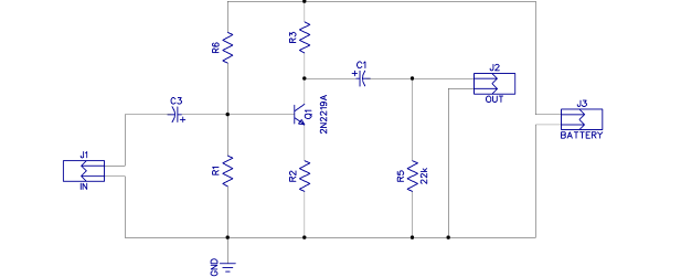
Example circuit diagram

The figure below, along with the 3D construction, illustrates the transistor amplifier wiring schematic. It is a promiscuous project, some of them in SMT with discreet components. The project contains elements, words, images, components, and more.

Example circuit diagram

Final Thoughts

Gerber Viewer Software for Windows is a software program that allows you to read and examine Gerber files (GRB files) using its comprehensive toolkit. Some of these applications are also the software for the Gerber editor so that you may examine and modify Gerber PCB designs. The program may export the file viewer in different formats, such as SVG, PDF, PNG, PDF, JPEG, etc. If you wish, you may also print out the design.

PNCONLINE equipped with big and sophisticated machinery, are used CNCs may accomplish the more advanced versions are devoted to a particular operation or all jobs simultaneously. These machines start producing PCBs instantly without being linked to a computer and also can interpret Gerber client files directly thus equipped with processors. Other kinds of equipment, always in accordance with the Gerber requirements, can conduct circuit controls and automated optical inspections (AOI).

Interested in getting your PCB design done on an urgent basis in New Jersey? Get it done at PNCONLINE.

Contact us at sales@pnconline.com