Tag Archives: turnkey pcb assembly

Printed Circuit Board

Printed Circuit Board Heat Sink Features/Functions

Heat management is essential for living on this earth as weather and devices affect buildings, vehicles, and equipment. Thermal management is also necessary for printed circuit boards, as they will get damaged if they can’t dissipate the heat their components generate. Besides, the board also gets hot due to soldering during manufacturing. Hence, heat dissipation methods become mandatory to increase the PCB speed.

Though FR4 is good at heat management, sometimes it is not enough when there is a high-speed circuit board. Likewise, the power supplies also generate heat and you have to install heat sinks and insulators. You must have experienced mechanical engineers to assess the heat flow to create a suitable heat dissipation system.

Printed circuit boards provide current to help devices function, but electronic devices get hot and heat sinks dissipate unnecessary heat. A PCB Manufacturer will use different heat sinks to prevent the overheating of PCB components and their damage, increasing the performance of the board.

Fourier’s law is an important law of heat that determines the heat sink function. When an element gets hot, heat travels from high-temperature areas to a low- temperature surface. The heat transfer occurs in three ways, such as:

  • Conduction
  • Radiation
  • Convention

When two components having different temperatures connect, it results in thermal conduction. In other words, fast molecules collide with slow molecules, resulting in heat transfer from hot components to cool components. PCB has high-temperature components like transistors, so you need to dissipate heat to cooling mediums, like water, air, or it can be oil, or some other element. This heat transfer occurs through conduction and convention.

Types of Heat Sinks

Heat sinks come up in different types as below:

Active Heat Sinks: There is a fan in an active heat sink to provide cooling. Such a heat sink provides great cooling, however, it needs regular maintenance as it is mostly running which affects its condition.

Passive Heat Sink: Passive heat sink is without a fan, so it remains still and needs less maintenance. You can consider it reliable and more effective than an active heat sink.

The shape and design also determine the type of heat sink, including swaged, stamped heat sinks, machining, folded and bonded fin, single fin sink, and forged heat sink.

Factors Affecting a Heat Sink

The main purpose of the heat sink is to exchange heat, so a large part of its surface area should be in contact with the cooling component like air. The quality of the heat sink depends on different factors, including its material, finishing, and certain physical features, like:

  • Air velocity
  • Attachment technique
  • Protrusion type

    Materials That Enhance Heat Sink Function

Manufacturers use specific materials to enhance the function of the heat sink in terms of heat transfer. These materials include:

  • Compounds
  • Conductive tape
  • Thermal paste

These materials are inserted between the surface of the heat sink and the surface of the component that generates heat. Metals having high thermal conductivity are ideal for heat sinks, including aluminum, copper, etc. But, aluminum is common as it is cheaper than others.

What To Consider Regarding Heat Sinks

Many factors affecting heat sink function include length, fin spacing and density, width, airflow, heat resistance, etc.

Which Devices Need Heat Sinks?

Electronic devices with components having poor heat dissipation ability need heat sinks. The devices in this case include multiple integrated circuits, diodes, transistors, switching devices, CPU and graphic processors, and LEDs.

Key Factors of Heat Sink Design

Heat sinks dissipate heat with the help of natural and forced convection, liquid, or radiation. The requirements of thermal management vary, depending upon the applications. Apart from a heat sink design, you have to consider several other factors while designing a thermal management system for a specific device. For like, you have to consider the standards of the component level, heat sink level standards, chassis levels, and requirements for a system level.

Let’s discuss essential factors that you have to consider during heat sink PCB design.

Heat Resistance: Thermal or heat resistance is the sum of multiple resistances occurring to heat flow between a cooling liquid and the die, thermal interference resistance, as well as the resistance between a moving fluid and a heat sink. Thermal resistance is bad for thermally unstable modeling systems.

The Value of Thermal Resistance: It is not precise, instead, it is approximate. It helps evaluate the thermal conductivity of the heat sinks and semiconductors. Heat dissipation depends on heat sink parameters that need proper analysis while designing the heat sink device. Heat sinks can be meshed through a 3D thermal resistance to have a complex system of thermal factors. Different platforms help design heat sink meshes.

Heat Sink Materials:  Generally, copper and aluminum are ideal heat sink materials as described above. These materials are good at conducting heat, especially copper as it also helps absorb heat, resists rust, and resist biofouling, moreover, it is also antimicrobial resistant. Though copper is better than aluminum, it is thick and costly compared to aluminum.

Another material is diamond and its thermal conductivity is also high due to the lattice vibrations it has. Some other materials for thermal applications include copper-tungsten pseudo-alloy, and AlSiC, Dymalloy.

Size and Shape of Heat Sink:  The shape and the size of the fins also help enhance heat dissipation. You can evaluate various fin shapes through modeling.

Fin Placement or Location: The arrangement of fins in a heat sink affects its cooling quality. Its configuration should be optimized to minimize the resistance of fluid movement, providing maximum air in the heat sink.

Cooling Quality: The cooling quality of the heat sinks has to be high. The aspect ratio of fins should be less to perform well. If the distance of the fin from the heat sink base is more, it will reduce the heat transfer to a cooling medium.

The function of the fins in a heat sink is to absorb heat from the electrical components of a device and sends it to the cooling medium. Besides, you should choose a cooling medium matching a PCB design and device requirements.

Heat Dissipation: Certain factors reduce the heat sink performance like a rough surface and gaps. They cause high resistance to thermal contact, thus affecting heat dissipation. You can reduce such thermal resistance by using thermal interface materials because most resistance-reduction techniques have limitations. You should consider specific things while selecting a thermal interface material, such as contact pressure, the material’s resistivity to current, and the dimensions of the surface gaps.

Attachment Methods: The attachment of the heat sink with PC Board components affects its thermal efficiency. So, you should choose the attachment technique carefully, considering the requirements of a thermal management system in terms of mechanical and thermal properties. Some popular attachment techniques include,

  • Thermal tape
  • Standoff spacers
  • Flat spring clamps

However, these attachment methods don’t end here as there are many others. You would also see m rein the future as engineers continuously update these methods according to new technologies.

By considering the above factors, engineers can design an effective heat dissipation system, including a heat sink.

Frequently Asked Questions

What Is Heat Sink?

The heat sink is a device and a way to manage heat in electronic products. Electronic components like transistors release heat, and you need heat sinks to dissipate heat to cooling mediums, like water, air, or it can be oil and other elements.

Do All Electronic Devices Need Heat Sinks?

Most devices need heat sinks to dissipate heat to cooling components. However, some electronic components have a built-in ability to dissipate heat. Generally, lasers or power transistors can’t transfer heat and need a solution to manage heat. MOSFETs and IGBTs are good examples in this case. So, here you need a heat sink device. 

Can PCB Survive Without Heat Sinks?

PCB components release heat which can damage them, making the electronic device slow. However, it also depends on the PCB materials as some have their heat dissipation property. Mostly you need a cooling system to enhance PCB performance. 

What Are The Types Of Heat Sinks?

The basic types in this case include the active heat sink system and the passive heat sink system. Some other types are also popular, like swaged heat sinks, stamped heat sinks, machining, folded and bonded fin, single-fin sinks, and forged heat sinks. 

Which Factors Influence The Heat Sink Design?

Many factors affect heat sink design, including its material, fin shape, and performance, fin size and location fin configuration, attachment technique of heat sink, and finally the thermal interface.

Final Thoughts

Devices having PCB also have heat sinks because they get hot due to high temperatures caused by different components. Heat sinks are either active or passive. You have to consider a few factors while designing the heat sinks, like its material, fin shape, and performance, fin size and location fin configuration, attachment technique of the heat sink, and finally the thermal interface. Various models help determine the heat sink parameters and geometry to provide a high-level heat transfer.

Would like to know more about the Heat Sink Features and Functions or pcb assembly services? Just Email us at sales@pnconline.com

Drill, Lamination, and Plating of PCB Design

Understanding Drilling

PC Board drilling involves different drilling machines which can make more than 30,000 holes in an hour. The machines have built-in systems for making precise holes and consist of spindles that can drill at a high speed of up to 110,000 RPM. An automated system and laser help manage drill bits to provide high-quality vias.

Drilling Of Through-Hole Vias

Standard PCBs have a through-hole where all PCB layers are drilled together under an NC machine. Then comes the plating of the holes’ inner and outer sides, and manufacturers use the same technique for all through holes, including the mounting holes.

Blind and Buried Via Drilling

The drilling of blind and buried vias occurs before lamination. The two-layered PCB goes through lamination after drilling. Whereas a multi-layer PCB is stacked and laminated after which it needs drilling and plating.

You can also make blind vias by drilling with a controlled depth where the drill machine works through the entire laminated board. Such a technique of making blind vias is cheaper than a sequential method, however, the hole size has some limitations. Besides, the routing of circuitry needs a specific technique.

Micro-vias Drilling

The drilling of micro-vias involves a laser machine because their size has to be small which is not easy to create through mechanical drilling. Micro-vias are ideal for thick PCBs, and you can connect them vertically by stacking them in layer pairs. Such as, in a traditional buried via, you can sequentially fabricate micro-vias whereas the buried vias need copper plating to connect the stacked vias.

When it comes to component holes, the through-hole technology works well. Such components are switches or standard connectors or mechanical components that need strong mounting that’s why the through hole suits them. Some common examples of devices having such holes include power regulators, resistors, op-amps, and capacitors, as they conduct heat and current.

How To Select A Drill

Though drilling is a basic function for a PCB Manufacturer, engineers use certain techniques to have precise drilling.

  • Sometimes a board needs lots of drills of the same size, which can cause changes in the bit during drilling. Such a change creates errors in terms of tolerance between hole diameters. So, engineers use drills of different sizes to avoid the quantity of the same-size drills.
  • Drilling diameter should be minimum, like in mechanical drilling, a six to eight mils drill is ideal for a 62-mils thick board. Whereas it is hard to use the small drill sizes in mechanical drilling, and its aspect ratio also makes plating difficult. So, engineers have to use laser drilling which is more expensive than normal drilling techniques. You have to use large drills for thick PCBs which are more than 62mils thick.
  • Use blind and buried vias when they are necessary otherwise avoid them. As their fabrication involves a sequential buildup method that increases the manufacturing cost of a raw board.

Different aspects affect the drilling methods and manufacturing cost of the PCB. Even the drill size affects the quality and cost of manufacturing. Too small holes highly increase a board’s cost, whereas too large holes can make assembly harder, increasing its cost. Engineers can avoid such issues by carefully designing a PCB, and having economical manufacturing.

PCB Plating or Metallization and Soldering

You need metal pads or lands to help components in mounting or soldering. You can’t solder the bare copper and have to plate it with an easy-to-solder material. In the past, lead-based tin was a common plating material. But, these days the environmental changes call for advanced materials like gold and nickel.

Unsoldered parts of the board need materials to resist soldering, such as polymer coating that prevents the bridging of traces. Moreover, it creates short circuits in the adjacent part leads.

Fabricating the External Layers

The above etching is ideal for circuits of external layers and the process includes drilling, metallization, and photoengraving. The final finishing happens after the external layers’ metallization. In general, the process includes soldering, silk screen application, testing, as well as packaging.

PCB Lamination

PCB lamination is crucial in terms of accuracy and creating a well-finished board. The process involves lots of stress, as you have to take care of the properties of PCB materials in terms of performance and production. PCB engineers and manufacturers have to work together to develop a functional product without sacrificing production.

Understanding the Lamination Process

The lamination of individual layers involves two main steps, such as:

Laying up:  It involves the stack-up of multiple layers. The manufacturer starts it from the bottom of the base substrate. Then comes the prepreg and internal etched layers. Then all layers are pinned together to make a final board without any disturbance. Laying up prepares the PCB before pressing.

Pressing of layers: Pressing involves heat and pressure that melts prepreg to finish the etched copper layer, making the insulation layers essential for electronic layers which can work closely. Prepreg bonds the layers, getting hard after curing, and makes a PCB mold.

You need to consider different factors during pressing. Like, many PCBs can be pressed together to save time and production costs. However, manufacturers have to place a separator between the individual layers to bear high pressure and heat without changing the PCB shape.

The laminating press also needs a vacuum to prevent the PCB voids to hinder the dielectric property, affecting its structural strength. The environment after pressing also needs consideration to prevent the STP quenching due to weather conditions. Manufacturers should store the pressed circuit boards in a press to cool them down. Cooling of the boards prevents the thermal contraction of the board.

Lamination Styles

Two styles are common in this case, such as:

  • Foil lamination
  • Cap lamination

PCB Lamination with A Foil: the foil lamination is simple and involves less hassle, as you have to foil the base and top layer. After lamination, the layers go through etching just like internal layers.  Foil lamination is more advanced than cap lamination, but you have to select the foil layer with care to remove them easily later on. The technician should work in alliance with the designer and material manufacturers to ensure precise production.

Copper Clad or Cap Lamination: It is an original method that PCB manufacturers have been using for years. There is a layer clad with copper between the base layer, top layer, and first and last inner layer. Such lamination is suitable for blind vias, however, you need a special laminate between the external and nearby layers to enhance a PCB function.

Purpose Of Sequential Lamination

You can use sequential lamination for advanced vias where drilling and plating come after lamination. However, vias other than through holes should be made before lamination, leading to sequential lamination. Such a technique involves many precautions in terms of materials and design to have a successful lamination. For like, you have to consider the z-axis CTE, Tg or glass transition temperature, and copper retention. A copper filling helps reduce copper accumulation to have a well-managed uniform CTE expansion.

The selection of the materials for PCB lamination involves great care. Besides, you should use the latest design software.

Testing a Final Product

Remember that PCB testing is very important to check damaged connectors and short circuits. Optical testing consists of layer scanning to find defects, whereas electrical tests involve a flying probe to verify different connections. It is easier to detect short circuits or breaks through electrical testing.  Whereas the optical inspection can better detect poor clearances between the conductors.

Final Thoughts

Drilling, plating, and lamination are important processes of PCB construction.  PCB drilling involves machines that can make more than 30,000 holes in an hour. The machines have built-in systems for making precise holes and consist of spindles that can drill at a high speed of up to 110,000 RPM.

An automated system and laser help manage drill bits to provide high-quality vias.  The two-layered PCB goes through lamination after drilling. Whereas a multi-layer PCB is stacked and laminated after which it needs drilling and plating.

The drilling of micro-vias involves a laser machine because their size has to be small which is not easy to create through mechanical drilling. Micro-vias are ideal for thick PCBs. Plating of the holes is also essential to provide electrical connections.

PCB laminating press needs a vacuum to prevent PCB voids to hinder the dielectric property, affecting its structural strength. The environment after pressing also needs to be considered to prevent any damage due to weather conditions.

Would like to know more about the Drilling, Lamination, & Plating or smt assembly? Email us at sales@pnconline.com

What’s a HDI Printed Circuit Board?

HDI stands for High Density Interconnect. HDI PCBs have finer traces and trace spacing, laser drilled micro vias and higher connection pad density. Its two chief advantages are that it permits the use of fine pitch BGAs and it reduces the number of PCB layers required because the finer traces and smaller vias allow more circuitry in a smaller area.

Narrow trace widths mean higher circuit density

At PNC standard PC Board fabrication uses a minimum trace width of 5 mil, with a 5 mil space between traces (5/5mil) PNC’s HDI trace widths can be as narrow as 3 mil with 3 mil spacing.  These finer traces allow 160% more traces in the same real estate. 3/3mil spacing will also allow two traces to escape between pads of a standard BGA, meaning less PCB layers are needed to fan out the pins from the BGA.

Microvias are the enabling technology for HDI

Narrow trace widths used in HDI PC Board are a result of the gradual refinement of photolithography and etching technology.  Microvias on the other hand, are a revolutionary innovation driven by the development of high powered lasers that can be controlled accurately enough to ablate a 3 mil hole through the surface layer of copper and underlying laminate, without damaging the underlying layer of copper.

The minimum hole size for PNC’s laser drilled microvias are 3 mil and the minimum pad diameter for the microvia is 7 mil.  Pads for laser drilled holes can be smaller than for mechanically drilled holes because of the location accuracy of the laser drilled hole.  There is no mechanical deflection of the drill bit to account for.  The laser drilled holes can be fully copper filled and planarized flat, so they can be used as pads for fine pitched BGAs with 0.4mm or smaller spacing. Using microvias as pads allows the signal trace to fan out by going straight down and out to an inner layer of the printed circuit board.

The biggest limitation with microvias is the aspect ratio of the holes.  Where a drilled through hole can have a 10:1 depth to diameter aspect ratio, a laser drill can achieve no more than around a 1:1 aspect ratio.  This means that the smallest microvia can only connect two adjacent copper layers. A larger diameter microvia can penetrate two layers. To connect deeper layers, the designer must stack vias one directly atop another.

Laser drilling of the microvias changes the way PCBs are fabricated and gives the designer flexibility that they do not have with through hole vias.  In a standard drilled PCB, via holes are drilled and plated after the PCB fabrication stack-up is completed.  Because the microvias can only bridge two or three copper layers, the microvias must be drilled and plated at each lamination step.  This means that microvias can be fully buried between layers, stacked or staggered to allow the microvia to connect multiple layers of the stack up.

The major space saving advantage of the microvia technology is that vias can just connect traces that need to be connected, rather than taking up real estate all the way through the PCB the way a through hole via does.

The Printed Circuit Board designers at PNC take advantage of this by locating the power and ground layers at the top of the stack up.  Since all active components access power and ground, sometimes through multiple pins, having the power and ground layers directly below the component layer allows all those connections to be made directly by microvias.  This leaves the component layers and layers beneath the power and ground layers completely unobstructed for signal routing. This has the added advantage of reducing parasitic capacitance because it eliminates the circuit stubs caused by plated through holes.

Two sided boards are typically fabricated with a combination of through holes and microvias.   Though holes can be drilled just through the core, connecting the stacks on the top and bottom of the board from the lowest layer, or through holes can be drilled through the entire stack directly connecting the traces on the top and bottom component layers.


HDI PCBs are a necessity when using fine pitched BGAs, but they can also reduce cost on PCBs without fine pitched BGAs because of the reduced layer count.  On your next PCB design, talk to the experts at PNC.  They can help you determine if HDI technology is can reduce your PCB cost by reducing layer count and shrinking the PCB size.

PCB assembly Pre-Reflow FAI

First article inspection (FAI) prior to SMT assembly is a design verification methodology that provides a reported verification and validation of details of a product on the shopfloor per its manufacturing procedure and requirements. There are various ways to perform FAI, from both supplier’s and customer’s side, making it a very dynamic process. This means that each organization can tailor its FAI method to benefit itself and consequently, its customer, yet maintain rigid performance standards at the same time. FAI involves qualitative and quantitative measurement. FAI is also highly effective since it can potentially fulfill process validation requirements of quality management systems like ISO9001 or AS9100.

In the PCBA manufacturing industry, FAI can be effectively employed in validating materials for manufacture, underlying technologies, manufacturing processes used, packaging, and equipment. It can also be applied to a batch of a given sample-size from a mass-production instead of just the first sample, as the name might suggest. At PNC, strict adherence to our manufacturing standards helps in production with better yield but at the same time, facilitating dynamic validation techniques in our manufacturing process allows us to reduce lead time. The focus of FAI in PNC assembly lies in validating the pcb assembly before reflowing so that the SMT team can make necessary adjustments for the next batch, saving time and effort during rework. They are also responsible for validating the correct loading of the right component in its allotted slot per the assembly program. This extra step helps in validating the placements of the components and improves the turnout rate for a successful production.

All aspects of reflow also must be amenable to improve solder performance and the same translates to our guideline where only the most recent batch of solder paste (with most activity) is permitted for use, which is validated by FAI. Apart from pre-reflow FAI, post-reflow X-Ray also helps validate the solder performance based on the reflow profile which can then be adjusted accordingly so that all components are successfully soldered. This can be similarly implemented at the rest of the printed circuit board assembly stages as well up to testing. But there is a necessity to establish a constant groundwork or point of reference in such a dynamic process to give each validation at a particular stage, the perspective of what changes were made before. This is achieved by using a single piece of documentation used to validate at every stage, wherever applicable, and that document reports any changes made to the processes or product, to the next stage.

pcb_assembly
pcb_assembly

PNC employs the use of AEGIS software to combine SMT assembly guidelines and inspection requirements into a single document (internally referred to as AEGIS). The AEGIS is used to report every single FAI validation to different stages of assembly. PNC’s FAI process for SMT starts with thorough solder paste FAI & its validation, which will be detailed in another post. For this post, let us consider pre-reflow FAI and highlight its validation process since it is the most crucial stage. The procedure is as follows:
1. The SMT team confirms the correct allocation of components as given in the assembly program. This is done by comparing each component with its description, measuring component value wherever applicable, and checking for physical marking on ICs. This helps in validating that the right component has been placed in its respective position on the board.
2. The next step involves checking for the polarity of components, wherever applicable. This is a two-step process. First, the supply angle of a component in the reel needs to be checked and second, the placement of that very component on the PCB needs to be verified.
3. Now, once the first board is assembled, the pcb assembly is put through FAI, where the placements of all components on the board are checked, any necessary placements that remain are placed manually and polarities of applicable components are checked and changed as per what is given in the AEGIS. The same changes are made in the assembly program to avoid the same occurrence in the rest of the batch. Components that are designated as DNP (Do Not Place) are also checked and finally, the solder paste information such as solder type, lot number, date of manufacture, and expiry are checked to ensure that the right solder paste has been used.
4. All these checks translate to notes, remarks, and checks on the AEGIS document, which can then be referred at later stages up to final inspection. If the job in consideration is a repeat job, it can be optimized to avoid any errors made in the first batch of production.
5. The board is then sent through reflow. Once reflowed, the board is extensively inspected under high magnification camera for quality of component placement, solder joints etc. yielded by SMT process.
6. Each section in the AEGIS is meant for FAI by a different team performing a different operation.

PNC has been able to reduce its lead time and increase customer satisfaction significantly and our personalized and successful FAI is a big factor contributing towards it. Further development to the FAI process is underway as much as it is needed to achieve better production yield over time for all the different types of PC Board assembly that are assembled at PNC.

CONFORMAL-COATING

CONFORMAL COATING

What is Conformal Coating?

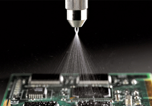
Conformal coating is protective chemical material coating applied after the final SMT PCB assembly or through-hole assembly process. Coatings are comprised of 5 different types, Acrylic, Epoxy, Urethane, Silicone and Parylene resins. Applying the coatings to a PCB board assembly can be done by hand spray, robotic spray, brush or dipping. The coating acts as an additional dielectric layer that provides protection due to environmental and mechanical stresses, such as thermal extremes, chemicals, dust, salt fog, abrasions, and moisture. In a PCB assembly that has close spacing of conductive pathways or close spacing of components the coating will help minimize dendrite growth over a period of time that causes shorting.

conformal_coating

Robotic Spray vs Traditional applications:

The method of application will depend on the customer requirements of the turnkey pcb assembly, but PNC prefers spray method for consistency in overall coating thickness. There are often select components on a pcb board assembly that will not be required to be coated. The traditional way is to block out or mask the selected components with tape. This is time consuming, costly and a possibility that the component can be damaged on the SMT assembly when removing. The robotic method can be programmed accurately to spray around the parts thus ensuring no component damage from masking and maintain a repeatable coating thickness.

When choosing a conformal coating for your turnkey pcb assembly, there are many manufacturers to choose from. The following are a few that we work with, Dymax, HumiSeal, Dow Corning, Hysol, Loctite, and Huntsman. Based on your application and environment of your PCB assembly, choose the Type of coating that fits the PCB board assembly, by visiting their web pages to find the strengths and weaknesses.

IPC J-STD-001D Conformal Coating thickness requirements

Type AR Acrylic Resin 0.03 – 0.13 mm (0.00118 – 0.00512 in)
Type ER Epoxy Resin 0.03 – 0.13 mm (0.00118 – 0.00512 in)
Type UR Urethane Resin 0.03 – 0.13 mm (0.00118 – 0.00512 in)
Type SR Silicone Resin 0.05 – 0.21 mm (0.00197 – 0.00827 in)
Type XY Parylene Resin 0.01 – 0.05 mm (0.000394 – 0.00197 in)