Tag Archives: Printed Circuit Board

PCB FABRICATION SUBSTRATES

PCB FABRICATION SUBSTRATES

What is PCB substrate?

Every home is required to have a solid foundation. A substrate is also required for every printed circuit board. The actual substance that contains the traces and elements is known as the PCB Fabrication substrate. The first step in creating a high-quality PCB is selecting the correct substrate. Structure and shape are required for a PCB. It also requires a platform or canvas on which to place all of its other components. The PCB’s performance is influenced by the substrate’s properties. A stiff substrate, for example, can improve the PCB’s strength and endurance. More design options are available with a flexible substrate.

The usage of a variety of substrates, ranging from solid fiberglass to flexible polymers, is becoming more common as the PCB industry evolves. Fiberglass has traditionally been the most prevalent type of substrate. It’s a low-cost, high-reliability material that gives the PCB a nice, stable foundation.
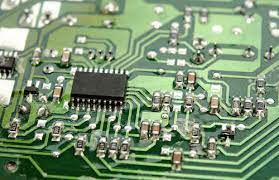
pcb board
pcb board

 Material of PCB substrate

It’s only reasonable that the materials you choose have an impact on your product’s performance. It’s the same with printed circuit boards, where selecting the correct PCB substrate materials can have a significant impact on the board’s performance, durability, and other characteristics.
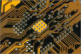
printed circuit board

Types of PCB substrate material

Following are the good material that we need for PCB substrate.

1. Copper foil:

PCB substrate materials are critical in defining the board’s endurance and quality. Manufacturers appear to be attempting to go towards fine lines and high density. You may be familiar with the term HDI PCB. This is the abbreviation of High-Density Interconnect Printed Circuit Board. To be classed in the HDI category ten years ago, a board had to have a line space (S) and line width (L) of less than 0.1mm. Today’s standards differ from one industry to the next. S and L on electronic devices are frequently set as low as 60m, and in advanced applications, they can even go as low as 40m. Once a thin copper foil substrate is applied, S and L can reach as low as 30m during circuit design development. The ideal thickness is between 9 and 12 meters.

The issue is that a thin copper-coated laminate can be costly and prone to flaws. It’s the most plausible explanation for why corporations use 18-meter-thick copper foil. However, if S and L are less than 20m, normal thickness copper foil may not be the best option.

pcborard
pcborard
 2. Dielectric Insulating Coatings:

The ability to build up is a key feature of HDI printed circuit boards. There’s a good probability you’ll be able to construct an appropriate circuit if you utilize resin-coated copper (RCC) or combine copper foil lamination with epoxy glass prepreg cloth. MSPA and SAP techniques have also been implemented by the manufacturers. By using an insulating dielectric film lamination with chemical copper plating, the copper conducting plane was created. The fundamental reason we can make acceptable circuits is because of the thin copper plane.

3. High heat protection and dissolution are required:

Electronic devices tend to generate more heat as the trend toward downsizing and high function continues; hence thermal management of electronic devices is becoming increasingly important. Thermal-conducting PCB research and development is one of the solutions to this problem. The main criteria for a PC Board to operate well in terms of heat resistance and dissipation are the substrate’s heat resistance and dissipation capacity. Improvements in thermal-conducting capabilities of PCBs are now being made through epoxy and filler additions; however this only works in a limited category. The most common way is to use IMS or metal core PCBs as a heating component. This system has several advantages over the typical radiator and fan, including a smaller amount and lower cost.

How to Select Substrate Materials for PCBs

You can choose between three distinct types of PCBs:

• Rigid
• Flexible
• Flex-rigid

The most important goal is to select a board that is ideal for your product. Many people strive for compact size and shape while overlooking performance. Polyimide film is a good choice since it is adaptable and can be used in a variety of applications, including black, white, and transparent. It also ensures a low coefficient of thermal expansion while keeping acceptable heat resistance. The Mylar substrate, on the other hand, is extremely flexible and resistant to external conditions. Furthermore, it is reasonably priced, which is why many consumers consider it. Flexible PCBs must attempt to achieve the same degree of frequency and speed performance as regular PCBs. Flexible boards can be made with advanced polyimide substrates and polytetrafluoroethylene.

Flexible boards are used in a variety of industries, including medicine, smartphones, and gadgets. As a result, the market has been implementing innovations in flexible and ultra-thin multi-layer boards (0.2-0.4mm). You can expect flexible boards to achieve speeds of up to 5Gbps at this time, but you’ll need to choose a substrate material with a low Dk/Df. It’s also a good idea to utilize conductors with a thickness of above 100m, as this will aid with current and power handling.

Best PCB substrate type

A substrate and printed wires are the two main components of a PCB (the copper traces). Substrates that divide the layers are required for multi-layer boards. The substrate works as physical support for the circuit components and printed wires, as well as providing electrical insulation between conductive portions. PCB Substrates are non-conducting materials. They act as a laminated electrical insulator between circuits for this purpose. An electrical insulator is a material that does not conduct electricity because its internal electric charge does not flow freely. As a result, plated through holes are used to connect traces on opposite layers on each layer of circuitry.

A substrate and laminate are commonly used as the foundation or base of a printed circuit board (PCB). The performance of the PCB is determined by the type of laminate and substrate used. As a result, choosing the proper types of PCB material for the job is crucial to getting the greatest results. Any PCB design guide should include such features:

 Working
 Durability
 Cost-effectiveness

The material you choose for your PCB can have an impact on its short- and long-term functionality, along with your contractor’s capacity to build it. You can’t blame the contractor if you buy substandard materials and they fail when your contractor tries to make the board. When maximum performance isn’t a must-have feature for a PCB, lightweight polyester material is typically a fine option. As long as lightweight polyester is utilized in conjunction with printed electronics (PE) technology, there are at least two reasons to choose it in these circumstances. Printed electronics with lightweight polyester have these features:

Cost-effective Lightweight polyester produces less waste, necessitates fewer manufacturing steps, and eliminates the need for desalination and purification.

Adaptability Flexible printed circuits (FPCs) are available, but the level of “bendability” that makes them so appealing is costly to accomplish. PE with lightweight polyester maintains flexibility at a far cheaper cost.

Traditional PCBs, on the other hand, is still the top choice for high-performance applications, and the materials used in their construction should be determined by the type of board required. For example:

 Manage frequencies ranging from 500MHz to 2GHz
 Allow for high power and, as a result, high temperatures
 Be “intense” and complicated
 Manage microwave and above-microwave frequencies

The board’s application decides the substrates and laminates to utilize to a considerable extent. There are five types of substrates, each with its own set of features for specialized purposes.

1. FR-4

Fiberglass substrates are comprised of woven fiberglass that has been impregnated with only a flame-retardant substance. The material is rigid and can be drilled, cut, or machined, although tungsten carbide tools are required due to the abrasive nature of the fiberglass. An FR-4 substrate is more resistant to cracking or breaking than an FR-2 substrate and is typically seen in higher-end devices.

2. RF
Low dielectric polymers are employed in RF substrates, which are used in printed circuit boards for high-power radio frequency applications. Despite its low mechanical qualities, the substrate exhibits remarkable electrical performance.

3. FR-2
This extremely low substrate is comprised of impregnated paper, also known as Phenolic, and is simple to the machine over a fiberglass substrate. Flame Resistant is denoted by the letter “FR.” This substrate is commonly encountered in lower-cost consumer devices.

4. Flex
Flex circuits are those that are meant to be very flexible or slightly flexible. As substrates, thin, flexible polymers are used. Although the manufacturing process is more complicated than utilizing rigid substrates, it provides benefits that rigid substrates cannot, such as reducing space by bending the circuit board to fit a specific place or where repetitive action is essential. A low-thermal resistance substrate is required for power electronics. A ceramic core or metalcore substrate has the essential properties to accommodate larger copper tracks and the high electrical currents that these circuit boards require.

Final Thoughts

Every substrate has its uniqueness and you get to know almost every substrate detail in this write-up. Interested to know more about our facilities at PNC? Contact us at sales@pnconline.com

SMT Assembly Technology

SMT Assembly Technology

Any piece of commercially manufactured electronic equipment these days is packed with tiny electronics. Instead of utilizing conventional components with wire leads, such as those used in home building and kits, these components are placed directly onto the boards’ surface, and many are very small.

What is Surface Mount Technology?

It is also known as SMT, Its a printed circuit board component installation process in which the components are mounted and linked onto the board’s surface utilizing batch solder-reflow procedures. Part leads are placed into plated through-holes and waves connected from the bottom, to fill in the holes and connect the components. Compared with plated through-hole insertion method, SMT offers the benefits of greater packing densities, better reliability, and lower cost. SMT is presently the most popular method for producing low-cost, high-volume consumer electronic assemblies.

Surface-mount technology is the name of the technique used for manufacturing an SMD. Most of the industry has moved away from using the traditional THT construction method of putting wire leads into holes on the circuit board to insert parts. Both surface mounting and through-hole mounting may be utilized on the same board for components that are not appropriate for surface inserting. Parts of SMT are often small than their through-hole frame since they have fewer or no lead.

Surface mount technology is used in almost all commercially produced equipment today since it provides substantial benefits during PCB manufacturing and allows much more electronics to be packed into a much smaller area due to the lower size of SMT components. Aside from the size, surface mount technology enables automated PCB assembly and soldering, resulting in substantial gains in dependability and significant cost reductions.

It is not necessary for component leads to travel through the board during PCB construction. Instead, soldering components directly to the board is quite acceptable. Consequently, surface mount technology was created, and the usage of SMT components grew quickly as the benefits of SMT components became apparent. In today’s electronics manufacturing, surface mount technology is the most often utilized technique for assembly. SMT components may be manufactured highly tiny, and several kinds, especially SMT capacitors and SMT resistors, are used in the billions.

SMT implementation on a PCB

The surface mount technology is used in the production of printed circuit boards. Surface mount technology refers to the assembly of electronic components by automated devices that put them on the board’s surface. In contrast to traditional PCB components, which are welded to the conductor, surface-mount components (SMT) are placed directly on the PCB surface, as is the case with conventional through-hole processing. When it comes to electronic assembly, SMT is the most widely utilized method in the business. In SMT assembly and production, surface mount technology is nearly entirely utilized. Surface mount technology allows more electrical components to be encapsulated in a small area.

Surface mount components are small and often perform well, and may be used with automated machines that select and place components, which removes the need for human involvement during the assembly process in many cases. Also difficult to install automatically, are the wire components since the wires must be pre-formed to ensure that the holes are spaced properly, and though in that case, there may be problems when the components are placed.

The majority of components on the circuit board are automatically positioned during PC Board fabrication. Some may need human intervention on rare occasions, although this is becoming less common. Some connections and other components have traditionally required supplemental installation, although manual placement is becoming less common. In today’s world, PCBs are frequently built to reduce or remove the issue make adjustments to incorporate parts that can be eventually put into the board.  Furthermore, several surface-mounted versions of components have been developed by component manufacturers, allowing for nearly completely automated production of most circuit boards. Technology using surface mounts PCBs must be selected with care, considering factors such as cost, electronic properties, or TGA (thermal expansion coefficient). During the development of a surface mount board (PCB), the kind of SMD element to be utilized dictates the type of PCB material to be used.

Pros and Cons of SMT

Pros

  • Better signal transmission:

The construction frequency may reach up to 5-5-20 solder joints per square centimeter when the PCB is bonded on both sides which are very high. High-speed signal transmission is possible with SMT printed circuit boards because of their short circuits and low delays.

  • Miniaturization:

Surface mount electrical components have a geometric dimension and volume much less than composite parts with through-holes. In general, through-hole interpolation parts may have their size and volume reduced by 60 percent to 70 percent, and few parts could have their size and volume reduced by 90 percent. Meanwhile, the weight of the components may be reduced by 60-90 percent.

Effect of high density:

The circuit’s distribution parameters are reduced because there are no or few leads on the element.

  • Less expensive materials:

Due to the improved efficiency of manufacturing equipment and lower packaging material usage, most SMT components cost less to package than THT components of the same kind and function. As a result, SMT components have a lower selling price than THT components.

  • Production method and cost:

There is no need to bend, shape, or shorten the components’ lead wires when placed on the Printed Circuit Board, which speeds up the process and increases manufacturing efficiency. The processing cost of the same functional circuit is less than that of through-hole interpolation, which may decrease overall manufacturing costs by 30% to 50%.

Cons

  • Repairs may be more challenging in small spaces.
  • It does not ensure that the solder connection will be able to resist the potting chemicals. When thermal cycling is done, connections may or may not be broken.
  • Although solder melts at high temperatures, components that produce much heat or carry many loads should not be surface-mounted.
  • This implies that parts that directly engage with the client should be physically bound to the hole rather than linked via it.
  • Since solder connections in SMT need less solder, the dependability of solder junctions becomes a source of worry. In this case, the development of voids may result in solder joint failure.
  • Surface-mounted components should not be used for components that produce significant quantities of heat or carry heavy loads because solder melts at high temperatures.
  • The majority of SMT component packages cannot be placed in sockets that allow for the simple installation and replacement of defective parts.

Method of surface mounts assembly

When electronic devices are placed to the surface of a printed circuit board using adhesive, surface mount technology is referred to as surface mount technology. It reflow solders the surface-mount assembly to the plate, essentially welding it together. Several components are selected during the design stage, and the printed circuit board (PCB) is produced using software tools, which prepares the ground for the surface mount assembly process to commence.

Preparation and examination of the materials:

Prepare the SMC and PCB and inspect them for faults. PCBs are often equipped with flat brazing pads, which are generally made of tin-lead, silver, or gold-plated copper and are referred to as pads.

Preparation of the template:

In solder paste printing, the steel mesh is utilized to hold the solder paste in a fixed location. It is manufactured in line with the layout position of the plate on the printed circuit board (PCB).

Print of solder paste:

The solder paste printer is the first piece of equipment to be placed throughout the production process. The purpose of this machine is to put solder paste to the suitable solder plate on the printed circuit board with a template and scraper. SMC and PCB solder pads are connected with solder paste using this method, the most widely used method.

Equipment’ locations:

Following confirmation that the PCB has the appropriate amount of solder applications, the board goes on to the next stage of the production method, which is assembling the parts. A vacuum or clamping nozzle is used to extract each component from the packaging. The visual system then checks the component before putting it at high speed in a preset location.

Inspection of the first component:

When it comes to first assembly or first piece inspection (FAI), subcontractors confront various difficulties, one of which is the time-consuming process of verifying client information. This is an important stage of the process since any mistake, if left undiscovered, may result in a significant amount of rework being required.

Soldering with reflow:

The assembled PCB board is subsequently transferred to the reflow welder for further processing, where it is heated to a suitable degree, allowing all of the electrical connections between the component and the PC Board to be established. This is done by bringing the assembly up to a suitable operating temperature.

Cleaning and Inspection:

After welding, thoroughly clean the board and inspect it for flaws. Rework or fix any flaws, then store the finished object. The most common SMT-related equipment and additional optical testing devices are SPI machines that are capable of being linked to the machine’s location to adjust the component position and connectable SPI machines that may be used to modify PCB alignment layouts when the printer is linked to it.

PRINTED CIRCUIT BOARD ASSEMBLY

Main aspects of the PCB industry – PCB Design, Manufacturing & Assembling

In this article, you’ll get to know the fundamentals of PCB manufacturers and how our company “PNC Inc.” is unique from other manufacturers in the United States.

What are the three main aspects of the PCB industry?

According to our experience of more than 50 years as the leading PCB Company in the industry, we can easily write that three main aspects in the PCB industry for which most clients look for are:

PCB Design
PCB Manufacturing
PCB Assembly

Design, Manufacturing, and assembling of PCB is a systematic method for examining the parts and components which is needed to execute. It included obtaining costs of a commodity and seeks to cut costs before actual development begins. There are specific manufacturing, design, and assembling principles required to be following during the PCB process execution of any electrical or electronics part. Eventually, a final design concludes the series with a review among the most common issues related to the PC Board or Printed Circuit Board.

Until continuous description, it is important to explain how the word ‘manufacturing design’ is used when speaking more generally and when talking more directly about PCB output. In general, design for manufacturing and assembling may lead to the simplification and optimization of a model or theoretical design in anticipation of their production. As these words are used to describe PCBs, they also imply a more straightforward study of possible production problems.

Ideal Design can Help PCB Fabrication:

The purpose of addressing the nature of manufacturing and assembling, in general, is to decide how a commodity can be produced and installed most cost-effectively. Manufacturing is to be done in a way to reduce the total cost and, more evidently, assembly design is required to be done to reduce commodity inputs, capital operating costs, and labor reduction. The emphasis is both on applying standards to lower manufacturing costs and also aim to shorten the product creation period. The fusion of these methods is often widely called manufacturing and assembly design for Mil-Spec PC Board.

Rules of PCB Manufacturer and Assembly:

After the conceptual Circuit Board Fabrication design has been developed, the company is required to research opting towards the most economical way of executing the PCB fabrication. The construction of a prototype or the development of a new version of a product could require a conceptual design. Once a conceptual design has been developed, a designer review will analyze the design’s bill of materials.

Try to use fewer parts in a design:

Reducing the number of components in PC board manufacturers is a simple aim with clear advantages. It would minimize construction costs and assembly difficulty, while not as obvious, it is of great advantage. When PCB assemblies are supplied using devices, for example, they are restricted to the number of modules they may be supported in a single port.

Being aware that if use many parts are used by pick and place machines in circuit boards fabrication will contribute to non-assembly. Cost savings are obvious. For example, if a design needs a resistance of 20K ohms, and 10K ohms resistance has been already used in the design, it might also be easier to use two 10K ohms resistors in sequence if this reduces the amount of time the computer picks and places simulation.

In the same way, you can speed assembly time up and transfer portions of the test requisites to the IC maker in search of regularly integrated circuits that can combine part of the specification into one IC. Having in mind the number and form of PCB components is perhaps the most significant move towards reducing total PCB manufacturing costs. In a term, the elimination of a component for the final design would decrease BOM costs, minimize purchase costs, production time, test time, and workload assembly feedback.

Use Original Components:

The use of composite materials will dramatically reduce construction time and expense. It goes without saying that defining a specific custom approach would significantly raise the initial cost of every product which may render a concept unfeasible. In addition, the use of more generic materials will shorten the supply chain of a commodity and mitigate supply issues. The fact that their measurements are easier checked until they are included in a PCB design specification is another advantage to prefer electronic interfaces.

Use Multifunctional Parts for Printed Circuit Design:

When an electric power part may be used for many uses in a model, the designer must take account of it. For instance, utilizing a container that can also act as hot in a design can give considerable cost control. A further definition of a dual-use mechanism through the use of a blockade as a link to ground from PCB board assembly.

Install all PCB Assembly Directions:

If practicable, all the board companies would plan all pieces to be assembled from the same side of an assembly around one axis. This is also referred to as a “Top Down” assembly in which all parts from top to bottom are placed. The use of this kind of single-sided assembly method saves time when a product is turned and rotated during assembly. As for all of the design choices, PCB design engineers would then have to consider whether producing a smaller PCB fabrication with components placed on every s sides of the board safer is compared with developing a larger PCB.

Advantages of PCB Manufacturers and Assembly:

• Fewer pieces ought to be handled and recorded.
• The expense of billing products should be minimized.
• The cost of handling can be reduced to some degree.
• Labor and input of electricity should be reduced.
• The total production period may be reduced to significantly increase manufacturing productivity.
• Lower sophistication results in greater efficiency.
• Increasingly competitive products should be.
• High Replacement margins are achieved.

The Circuit Printed Boards Manufacturers and prototype PCB manufacturers should have a simple way to reduce the next design bill. The advantages of reducing the number of designs are evident. Materials will become more viable as they are cheaper and less vulnerable to loss, however by lowering the number of materials used in the production of product costs, paperwork needs will be decreased and the work required for SMT assembly. All these factors contribute to lower manufacturing costs and encourage either better commodity or price profits at more affordable prices.

In addition, the processing period is shortened so the goods can be delivered to customers in less time. An optimal printed circuit board may be built with the right PCBA assembly considering all the above implementation of these objectives.

At PNC Inc., You’ll get your PCB done from any of the following design tools of your choice as we have an in-house facility available for all the tools.

• Cadence Allegro v16
• OrCAD Capture v16.3 & OrCAD PCB Designer v16.3
• PADS v9
• Signal Integrity Analysis: Hyperlynx

You will get the following deliverables from us:
• Gerber, drill files & PCB File
• Assembly and fabrication files
• Formal drawings on your (client) desired format

Why you should choose us & why we are better than others in the Market?

At PNC Inc., we have got the facility of executing all the design, manufacturing, and assembling in the same building. In this way, you don’t have to visit different places to check the progress of your work. You’ll get all the things done in the same building at our Nutley, New Jersey facility. That’s why we are a “one-stop-shop” and providing all the services under the same roof.

Work with PNC to Reduce PC Board Costs

When it comes to reducing the manufacturing cost of a PCB, it is important to remember that a significant part of the cost of a PCB assembly is already baked in at the design concept stage.  The product concept defines the PCB size and shape, while the performance of the system dictates the microprocessor, memory and other functional elements of the circuit.

However, some of the assembly cost can still be affected by design choices made by the PCB designer.  A PCB that is designed for manufacturing (DFM) can reduce both the fabrication cost of the PCB and the costs of component assembly and soldering. A DFM approach to design can also reduce the likelihood of the hidden costs of poor yield in production.

The best way to achieve the lowest cost, most manufacturable design is to work closely with the prospective  manufacturer, since the way to maximize DFM cost savings is to design for a manufacturer’s specific equipment and technology, rather than to rely on general rules.

Reducing PCB Fabrication Costs

The first step to reducing costs in PCB fabrication to reduce the number of operations performed by the manufacturer.  The second step is to optimize the PCB design to leverage a manufacturer’s particular fabrication technology.

One way to reduce costs is to eliminate or minimize the amount of machining required around the board edge or within the PCB itself.  Rectilinear PCB outlines without internal slots will minimize machining, and the rectangular shape allows the PCB to be grouped in larger panels that are separated after assembly.  These large panels streamline assembly by allowing a several PCB to go through component assembly and reflow at the same time, improving throughput. For example, PNC can process a maximum panel size of 18” X 24.” To ensure that the components on the PCB are not damaged during the scoring and separation from the panel, components should be kept 200 mil from the board edge.

Reducing board layers to reduce fabrication costs

The generally accepted rule that reducing the number of PCB layers in a stack-up will reduce cost has become more complicated with the advent of HDI technology.   The reason is that the cost of an additional Printed Circuit Board layer is not linear, so a cost calculation needs to be made for each jump in the number of layers. Is it cheaper to use finer trace widths and buried vias to reduce the layer count from six to four?  Only the manufacturer is going to know.  However, as a board gets past eight layers costs increase non-linearly with each additional layer.  The aspect ratio of the through hole vias begin to become a factor, as well as the sheer number of vias that need to be drilled and plated to connect all those layers.   At an eight layer stack up or above, the additional cost of HDI technology begins to make economic sense if it is used to reduce the number of stack-up layers required.

Respect drill to copper clearance and aspect ratio design rules

Respect the design rules for hole sizes and hole to copper clearance.  If the real estate on the PCB allows it, selecting hole sizes clearances and annular ring sizes larger than the absolute minimum will improve fabrication yield. Here are the through hole design rules for PNC:

Non-Plated Through Hole (NPTH)
● Finished hole size (minimum)= 0.006″
● Edge to edge clearance (from any other surface element) (minimum)= 0.005″
Plated Through Hole (PTH)
● Finished hole size (Minimum) = 0.004″
● Annular ring size (Minimum)= 0.004”
● Edge to edge clearance (from any other surface element) (minimum) = 0.009″

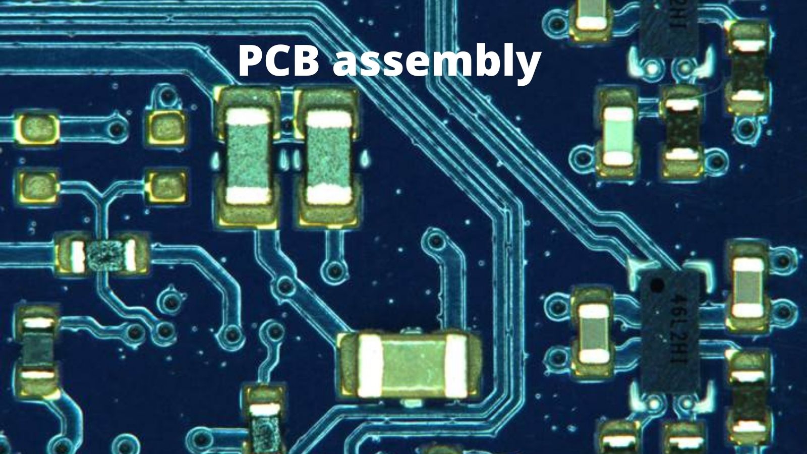
PCB assembly
PCB assembly

Reducing PCB Assembly Costs

To reduce assembly costs the objective is the same as reducing PCB fabrication costs; reduce the number of operations, and optimize the PCB design to leverage a manufacturer’s particular fabrication technology.

One easy way to reduce assembly costs is to stay away from the smallest passive packages.  0603 passives are easier to place than 0402 or the almost invisible 0201.  If possible, chose active parts that have leads rather than ball grids, because they are easier to place, they can be visually inspected instead of x-rayed, and they are easier to rework.

Avoid parts that have to be manually soldered.

Manual operations are always expensive, and the designer should do everything they can to avoid the need for them.

Component manufacturers have recognized this and now offer through-hole components (typically connectors) that can be reflow soldered.  This technology called “Through-Hole Reflow” allows through-hole components to be soldered in the same reflow process as the SMD components, eliminating a pass through the wave soldering machine or manual soldering.

Finally, if possible, avoid putting components on both sides of the board.  The cost of a higher density PCB with components on one side may be cheaper than a lower density PCB with components on both sides.

Don’t wait until the PCB design is finished before talking with PNC

The best time to talk with the PC Board design experts at PNC is early in the layout process.  They can tell you when to use HDI to reduce costs and can advise on how to optimize panel size. The experts in the assembly department can also work with you to select components that will reduce assembly costs and increase yield.

Give PNC a call today.

PCB Design, Selecting the Right PCB Trace Widths?

Every PCB designer has a series of decisions to make PCB Design as they translate an abstract schematic into a functional, reliable, and manufacturable PCB assembly. Placing the components on the    PCB is usually the first step, connecting those components with copper conductors to create the circuit is the next.  To connect the components, the layout designer must interpret the circuit netlist and turn that netlist into actual copper traces, subject to constraints of both manufacturing technology and the laws of physics.  One of the most important considerations for the designer is the appropriate trace width for each of those connections. The width of each trace determines both the real-world performance of the circuit and the overall size and number of layers of the PCB.

To balance circuit performance and PCB size, the designer needs to balance four considerations:

  • The manufacturer’s minimum trace width and spacing
  • The size and pitch of the component pads that the trace will connect
  • The amount of current flowing through the trace
  • Whether the trace is part of a controlled impedance circuit

Minimum Trace Width and Spacing

The manufacturer’s minimum trace width and trace spacing will define the smallest trace width that can be used for all signal traces that do not carry significant current or have impedance constraints.  The minimum trace width is typically used as the default for the layout, since using the minimum trace width will result in the smallest possible PCB and the most flexibility in routing.

For a standard Printed Circuit Board, fabrication minimum trace widths/spacing is typically 5 mil (.127mm). PNC’s High Density Interconnect (HDI) PCB trace width/spacing can be as narrow as 3 mils (.076mm)

Trace Width vs Pad Width

Another consideration when selecting trace widths is that the trace should be smaller or equal to the pad width. For the most part, if working with the minimum trace widths, this will not be an issue, however, care must be taken when laying out the traces and pads for high current applications.

High Current Traces

Once a designer has placed the components in the layout, they will often focus next on creating the power and ground traces to the active components.  This is because the current carrying traces need to be appropriately sized and routed.   Signal traces, which are typically at the minimum trace width, can be more easily routed around the larger power traces.

Copper PCB traces, like any conductor, have an internal resistance that is proportional to the conductor length, and inversely proportional to its cross-sectional area. Since the copper on a layer is of a uniform thickness, the width of the trace determines its cross-sectional area.  There will be both a voltage drop along the trace as well as heating of the trace due to the power dissipation.  If a PC Board trace is not sized appropriately to carry the current required by the circuit, the trace can fail due to overheating, or the high voltage drop along the trace can cause intermittent circuit problems as the current and thus the voltage drop in the trace varies over time.

Designers often create an internal copperlayer with multiple buses of various voltages.  Since that layer consists only of power busses, the buses can be quite wide.  The designer will then connect the individual components to the bus using vias rising to the component’s power pins.  A bus based design reduces voltage drop at far from the power supply while reducing the width of the short connector trace to the same size as the component pin pad.

In the days before the internet and sophisticated PCB layout software,  designers would use the pages of current vs trace width tables  in IPC 2152 “Standard for Determining Current Carrying Capacity in Printed Board Design”  Now there are online calculators  based on those tables that take in to consideration all of the factors involved in determining the appropriate trace width for a specific current and allowable temperature rise of the trace due to the power dissipation. Many full featured Printed Circuit Board layout applications have the calculations embedded in their design rules.

If a PCB is intended for high power applications such as motor control or an LED power supply, a copper layer thicker than the typical 1 oz can be used but note that it is difficult to etch fine traces and pads in thicker copper.  Make sure to check with the PCB fabricator about their capabilities. PNC has experience with thick copper layers and can provide advice to the designer about what is possible.

Controlling Trace Impedance

The last consideration in selecting trace widths is the impedance of the trace, which becomes a factor in high frequency signals such asDDR busses, video such as HDMI, and high speed serial communication like USB and Gigabit Ethernet. At these high frequencies, not only the trace resistance, but the capacitance and inductance of the trace become significant factors.

Designing controlled impedance (CI) circuits is beyond the scope of this post, because designing a controlled impedance circuit requires taking into account the dielectric constant of the PCB, the length and routing of the trace in addition to the width of the trace.  However, trace width is one of the most easily controlled elements of impedance controlled circuits,so the trace width on individual controlled impedance circuits may be different from the width of other low frequency signal traces, and those traces may be finetuned after the prototype PCBs are tested.

The design of controlled impedance circuits is described in detail in IPC-2141A “Design Guide for High-Speed Controlled Impedance Circuit Boards”, and many of the formulas are available in online calculators or as options in PCB layout applications. When designing high speed circuits, it also pays to work with a PCB manufacturer like PNC that has expertise in fabricating PCBs with precise and consistent dielectric properties.

Schedule a Design Review with your PCBA manufacturer

 The designers at PNC have experience with both high power and high-frequency RF and microwave PCB layout designs.  Because they work closely with the manufacturing team, they know what is possible to achieve with the thick copper layers used in today’s compact LED and motor controllers,  and they know what it takes to maintain consistent dielectric properties in the substrates, needed for predictable RF performance. Let them help you with your design.