HDI stands for High Density Interconnect. HDI PCBs have finer traces and trace spacing, laser drilled micro vias and higher connection pad density. Its two chief advantages are that it permits the use of fine pitch BGAs and it reduces the number of PCB layers required because the finer traces and smaller vias allow more circuitry in a smaller area.
Narrow trace widths mean higher circuit density
At PNC standard PC Board fabrication uses a minimum trace width of 5 mil, with a 5 mil space between traces (5/5mil) PNC’s HDI trace widths can be as narrow as 3 mil with 3 mil spacing. These finer traces allow 160% more traces in the same real estate. 3/3mil spacing will also allow two traces to escape between pads of a standard BGA, meaning less PCB layers are needed to fan out the pins from the BGA.
Microvias are the enabling technology for HDI
Narrow trace widths used in HDI PC Board are a result of the gradual refinement of photolithography and etching technology. Microvias on the other hand, are a revolutionary innovation driven by the development of high powered lasers that can be controlled accurately enough to ablate a 3 mil hole through the surface layer of copper and underlying laminate, without damaging the underlying layer of copper.
The minimum hole size for PNC’s laser drilled microvias are 3 mil and the minimum pad diameter for the microvia is 7 mil. Pads for laser drilled holes can be smaller than for mechanically drilled holes because of the location accuracy of the laser drilled hole. There is no mechanical deflection of the drill bit to account for. The laser drilled holes can be fully copper filled and planarized flat, so they can be used as pads for fine pitched BGAs with 0.4mm or smaller spacing. Using microvias as pads allows the signal trace to fan out by going straight down and out to an inner layer of the printed circuit board.
The biggest limitation with microvias is the aspect ratio of the holes. Where a drilled through hole can have a 10:1 depth to diameter aspect ratio, a laser drill can achieve no more than around a 1:1 aspect ratio. This means that the smallest microvia can only connect two adjacent copper layers. A larger diameter microvia can penetrate two layers. To connect deeper layers, the designer must stack vias one directly atop another.
Laser drilling of the microvias changes the way PCBs are fabricated and gives the designer flexibility that they do not have with through hole vias. In a standard drilled PCB, via holes are drilled and plated after the PCB fabrication stack-up is completed. Because the microvias can only bridge two or three copper layers, the microvias must be drilled and plated at each lamination step. This means that microvias can be fully buried between layers, stacked or staggered to allow the microvia to connect multiple layers of the stack up.
The major space saving advantage of the microvia technology is that vias can just connect traces that need to be connected, rather than taking up real estate all the way through the PCB the way a through hole via does.
The Printed Circuit Board designers at PNC take advantage of this by locating the power and ground layers at the top of the stack up. Since all active components access power and ground, sometimes through multiple pins, having the power and ground layers directly below the component layer allows all those connections to be made directly by microvias. This leaves the component layers and layers beneath the power and ground layers completely unobstructed for signal routing. This has the added advantage of reducing parasitic capacitance because it eliminates the circuit stubs caused by plated through holes.
Two sided boards are typically fabricated with a combination of through holes and microvias. Though holes can be drilled just through the core, connecting the stacks on the top and bottom of the board from the lowest layer, or through holes can be drilled through the entire stack directly connecting the traces on the top and bottom component layers.
HDI PCBs are a necessity when using fine pitched BGAs, but they can also reduce cost on PCBs without fine pitched BGAs because of the reduced layer count. On your next PCB design, talk to the experts at PNC. They can help you determine if HDI technology is can reduce your PCB cost by reducing layer count and shrinking the PCB size.
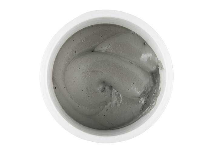
Solder pastes are amorphous putty-like soldering materials used to solder surface-mounted components to the Printed Circuit Board. The effect of solder paste on the PCB’s structural and functional integrity is the paramount factor to consider when deciding on selection of solder paste for application. Many factors which contribute towards the strength of the solder joint and its conduction efficiency need to be addressed as well. This is not just a discussion on what measures and precautions to take during PCB assembly and reflow, but also to put into question what a PCB design engineer should consider when designing a PCB and how the layout should adapt to the corresponding solder paste properties to yield the best result. It is a very brief introduction towards an expansive topic like solder pastes which will be discussed in further detail in future posts.
PROBLEM STATEMENT
A big concern for manufacturers arises when they need to select the right solder paste for SMT applications that is best suited to the PCB assembly and the manufacturing setup. A regular PCB has different types of components, all of which cannot always be compatible with the one solder paste applied across the board and thus, need some necessary compromises in solder selection. PCB designers should be educated about solder paste application and properties in SMT manufacturing to increase reliability of product yield.
SOLDER PASTE BASICS
Solder pastes are categorized based on the following characteristics: RoHS compliance (solder composition), flux type, grain size etc. RoHS (Restriction of Hazardous Substances) is a directive which mandates the exclusion of lead and other hazardous materials from solder pastes and manufacturing processes and aims to reduce environmental and occupational hazards related to electronics manufacturing. It has been adopted as a standard for commercial applications while only military applications can use leaded manufacturing processes. Many components now specifically require RoHS or non-RoHS procedures for PCB Assembly.
Flux is a chemical resin that is used to facilitate the soldering process. It is responsible for removing dirt and preventing oxidation of the component tips during reflow. They can be classified as either water-soluble fluxes or no-clean fluxes. Water soluble fluxes can be cleaned by using water while no-clean fluxes produced low levels of residue which are not necessary to clean but it is advised to clean with designated chemical wash to provide better result.
Solder pastes consist of solder grains which are available in different sizes which are given numerical designations from Type 1 to Type 8 based on descending order of solder grain sizes. Decrease in solder grain size also highlights the advancements in solder technology where Type 1 was adopted first, and Type 8 is the latest addition to minimum achievable solder grain size.
SOLDER PASTE
Since 2006, commercial solder pastes were manufactured and used without lead and other hazardous materials like cadmium and mercury in accordance with the RoHS directive. The directive also affected key PCB fabrication processes and successfully eliminated usage of hazardous materials for commercial applications. Lead in a traditional tin-lead alloy solder is responsible for lowering the melting temperature of the solder to approx. 183°C and it also helps slow down the rate of tin whisker growth in electronics. The process of finding replacements to maintain those advantages offered by lead is still ongoing. Lead-free solders have higher melting points and are more expensive than leaded solders.
The most popular lead-free solder currently being offered is tin-silver-copper alloy which has a melting temperature of approx. 217°C. This has also resulted in components like resistors, transistors being conformed to RoHS compliance. The main drawback of maintaining RoHS compliance for the product is that it is significantly more expensive than leaded processes and does not yield any benefits of switching to lead-free options. The effect of RoHS directive on component manufacturing and the larger effect on electronics manufacturing will be discussed in detail in future posts.
As of today, Type 3 solder is the most widely used solder paste. The following comparison consists of certain superficial characteristics which are a good point to start at before diving into a thorough discussion for each and exploring more complex properties and features of solder pastes. The reason behind comparing T3, T4 and T5 specifically is that T4 and T5 were recently adopted for mass usage for finer and smaller footprints in the PCB assembly industry while T3 has been the industry standard for a long time.
solder paste
It is important to note that the sensitivity and reactivity of solder paste to temperature change increases as the solder grain size decreases. This is due to increase in the number of solder grains occupying the same area as the solder grain size decreases. Simply put, the greater the number of solder particles in a given area, the more reactive that particular area of solder will be. Therefore, from this we can conclude that T4 solder will melt at a lower temperature than T3, and T5 will melt at a lower temperature than T4. The advantages, disadvantages and the various effects of using small grain-size solders on component structure and performance will be discussed in further detail in the next post.
FLUX
Fluxes are infused in the solder paste and they are released during reflow. The flux is always released before the solder can melt to provide an oxidation-free environment. Its chemical profile consists of a natural or synthetic resin to coat the component pins and pads, activators to release the flux at the right temperature, solvents to facilitate deposition of solder on the joint, and additives to compensate for any modifications in flux composition. Water-soluble and no-clean fluxes are both used in various situations based on the amount of oxidation occurring during reflow, the level of reactivity of the solder, solder grain size, material of the board, and surface finish of the board.
No-clean fluxes are generally used for boards where the corrosion resistance of the surface is weak. It yields low residue on the printed circuit board assembly because the flux either burns off during reflow or it forms noncorrosive, localized residue around the solder joints. Contrary to its name, it does require cleaning post-reflow but less so than most other high-residue fluxes. No-clean solder pastes are used as an industry standard by most electronics manufacturing service providers because of its ease of use. The main drawback of using no-clean flux is that since it is less corrosive, it does not provide as much protection from oxidation as water-soluble flux but that has to be accepted as a trade-off for better quantitative results in large-scale production.
Water-soluble fluxes are generally used for precise action and give excellent results but the main drawback is that they require careful application and condition regulation due to their highly reactive and corrosive nature, and the difficulty in cleaning them post-reflow. Compared to no-clean flux, it produces more residue that cannot be removed easily from the board and due its high corrosivity, it may damage the PCB surface and component leads. Cleaning unwanted residue off the board requires additional machinery which occupies valuable space on the shopfloor. This limits its usage in the industry to only customer requests or specifications to use water-soluble solder pastes.
KEY CONSIDERATIONS FOR PCB DESIGNING
It is important to consider how solder selection will affect your PCB design. For simplicity, the effects will be divided based on solder paste composition, solder size and flux usage. Many of these considerations may overlap or may have to be used in conjunction for achieving the best result.
SOLDER PASTE COMPOSITION:
• Components used on PCB should be first checked to see if they are RoHS compliant or not, based on the solder paste used. Components with RoHS compliance usually have different leads which may or may not be compatible with leaded solders, and it may affect the solderability of the component to the copper pads, the solder joint’s mechanical strength, and component shelf-life and performance. It is also important to ensure the components operating and manufacturing parameters meet the solder paste properties, otherwise components may get burned or dysfunctional during the reflow process, leading to visible or latent component failure.
• Flux selection should be based on solder paste composition. Flux release at specific temperatures should be done in conjunction with the reflow profile for that specific solder paste. Solder melting and flux activation occur at different instances in the reflow process. Early activation of flux may cause surface corrosion, component failure, early burn-off which may lead to poor soldering and late activation may lead to increased oxidation during reflow process along with difficulty in cleaning.
SOLDER SIZE
• Solder grain size should also be considered when choosing component package and its corresponding design footprint on the Printed Circuit Board. Larger footprints do not require smaller grain-size solders. If the grain size is small, say T5, then based on its high reactivity, more number of particles per unit area and greater wetting ability, solder may flow too easily on melting resulting in solder defects which will affect component performance and product life-cycle. The reverse situation, where small footprints are used in conjunction with large grain-size solders, also leads to solder defects.
• Component package selection will also affect stencil aperture size, stencil thickness and solder deposition efficiency. Using large-size solders, say T3 solder, for micro-BGA or 01005-imperial sizes will result in gasketing and insufficient paste deposition; while using small-size solders, say T5 solder, for large footprints may result in bridging.
• The spacing between footprints of separate components, spacing between component leads of the footprint on the Printed Circuit Board should change based on the solder grain-size as using large grain sizes for small footprints, and vice versa, will lead to solder bridging which will in turn affect device performance and life-cycle.
FLUX COMPOSITION
• PCB thickness, material and coatings should be selected based on flux used for the reflow process. One should avoid using water-soluble fluxes for a thin PCB as they are highly corrosive in nature and may lead to excess surface corrosion. Corrosion resistant material and coatings should be used in accordance with the flux selected, as not using them will lead to corrosion and cleaning issues and using them when not needed(say a no-clean flux is being used) will increase cost of production.
All PCB’s should be designed keeping in mind the effects of solder paste, stencil design, flux, process used on
SMT assembly PCB’s. Some of these topics and more will be added to the list and discussed in further detail in the future.
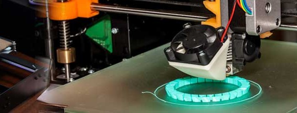
The time from concept to prototype has accelerated remarkably in the past decade. 3D printed prototype components in a wide variety of materials are available in hours. Machined or sheet metal components are available from rapid prototype shops in only one or two days.
Prototype Printed Circuit Board Fabrication and assembly companies like PNC have followed this trend towards faster prototypes and can now provide complete assemblies in less time than ever before. PNC can fabricate and deliver a bare 10-12-layer PCB in just three days, and a simple double-sided board in just 24 hours.
However, even with the streamlining of PCB fabrication, the fully assembled PCBA is often the longest lead component in prototype designs primarily because of the sheer number and variety of passive and active components to be purchased and the demands of accurately placing and soldering those components. Sourcing the components on a typical PCBA BOM can take days in the best case and weeks in the worst case. Setting up and running the assembly job can add another few days, especially for double sided PCBs, and PCBs with a combination of surface mounted and through hole components.
Fortunately, there are some things that a product development team can do to reduce PCB assembly lead time.
First, do everything possible to reduce the impact of long component lead times. Plan to order the components as early as possible in the circuit design process. Deciding when to order components requires balancing the costs of scrapping some components as the design matures vs. the benefits of reducing the lead time for an assembled PCBA by days or weeks.
Second, reduce the time required to set up and build the prototypes by working with a full-service company like PNC. PNC has the capability to both fabricate the bare PCB and assemble the components. This means that the PCB fabrication team and assembly team can save time by working in parallel. While the PCBS are being fabricated, PNC’s engineers can create pick and place data, solder paste stencils and program the assembly equipment. When the PCBs are finished and the components arrive, everything is ready to begin assembly immediately.
The third way to save time with PCB prototypes is to minimize the number of PCB prototype iterations. Saving a full printed circuit board assembly prototype cycle is the most effective way to reduce the time from concept to mature design.
One way to reduce design iterations is by testing circuit designs as early in the design process as possible by building “Works Like” prototypes. “Works Like” prototypes are usually combinations of development kits, large one or two layer PCBs with larger SMT components that can be soldered by hand and various types of breadboards. In addition to testing the circuit, a “Works Like” prototype gives software developers an early platform to start developing code and debugging the circuit design. The result of testing early with rough prototypes is that you fix problems before you have invested the time in the full layout and prototyping process.
In parallel, the mechanical engineers can optimize cable routing and connector placement by printing 3D models of the PCBs, then epoxying actual connectors to the board model. This is an effective way to quickly try different options for cable routing using actual cables and connectors, since it is difficult to simulate the way actual cables behave with CAD software.
Experienced electrical engineers know that it is often poor connector access or cable interference that drive Printed Circuit Board layout redesigns as often as issues with actual circuit performance.
Once the circuit has been tested with the “Works-Like” prototype, and the board layout has been tested with 3D printed models, the last way to save time is to work closely with the PCB manufacturer to make sure that the PCB fabrication files are clean and complete, and that the BOM is accurate and matched with the circuit and layout to avoid placement mistakes.
This is another reason to select a full-service prototype pcb manufacturer like PNC. PNC can be a partner during the layout and design process, though fabrication and assembly ensuring the final design can be translated into a working prototype in the least possible time.