Tag Archives: pcb assembly services

Minimizing Crosstalk in PC Board Layout

In this ongoing series on PCB layout from the design team at PNC, previous posts have looked at some of the initial steps to turn a circuit schematic into a manufacturable, reliable PCB. These posts have looked at  component placement, selecting appropriate trace widths, and BGA routing.   In this post we are going to take a deeper dive into methods for reducing crosstalk in the PCB design. After the power and ground have been routed, the next task is to route high speed signal traces, and the traces that could either generate or receive crosstalk.

 What is Crosstalk?

Crosstalk occurs when the signal on an aggressor trace on a PCB appears on a nearby victim trace, due to capacitive and inductive coupling between the two traces.  Typical aggressor signal traces are:

● High speed digital signals, especially clock signals
● Noise from switching power suppliers
● High frequency RF.

Victim signal traces, on the other hand, carry high impedance signals like op amp input lines or reset lines, or low impedance signals with long loops.   Low amplitude signals such as a sensitive analog measuring circuit traces are also susceptible.

Crosstalk occurs when aggressor trace and victim trace are close together and run in parallel for a distance.  The aggressor and victim(s) can be side to side on the same layer or on top of each other on adjacent signal layers. Coupling between traces on adjacent layers separated by just a thin section of laminate is called broadside coupling.
Minimizing Crosstalk in PC Board Layout


Printed Circuit Board Design guidelines to reduce crosstalk

There are several design rules to reduce crosstalk between signal traces.  Before applying these rules, the first step is to use the general guidelines described above to identify and flag any potential aggressor signal traces and their potential victims.

Since crosstalk occurs between two traces running in parallel, try to reduce the distance that the aggressor and victim traces run in parallel. Unfortunately, this may be difficult if the signals originate and terminate from the same locations.  To minimize broadside coupling try to orient the signal traces east-west on one layer and north-south on the second layer.

It is essential to have a broad contiguous ground plane directly under (or over) the signal layer.  A ground plane located between two signal layers can prevent broadside coupling. However, make sure that ground planes located on adjacent layers but not electrically connected do not overlap.  The overlapping ground planes separated by a dielectric form a capacitor, which can transmit noise from one ground plane to the other. This can defeat the purpose of separate ground planes if they were created to isolate the noisy elements of a circuit from the noise sensitive ones.

Increasing trce spacing

The most effective method of reducing crosstalk is to increase the spacing between the aggressor signal trace and the potential victim traces.  Like all electromagnetic radiation, electrical or magnetic coupling between the two traces drops with the square of the distance between them.  The amount of spacing required between the traces is dependent on the height of the traces above the ground plane.   The formula defining this relationship is from Douglas Brooks “Crosstalk Coupling: Single-Ended vs. Differential”   The coupling between two traces is proportional to:

Where S is the spacing between traces, and H is the distance from the trace to the ground plane.  Once H is defined by the lamination stack-up, the relative change in coupling can be easily plotted as a function of S.  Douglas Brooks looks in detail at the coupling between traces under several scenarios.  For those looking for some general guidance, a spacing of 5H is considered conservative.  The PC Board design team at PNC can assist designing a PCB stack up that will minimize the spacing needed between coupled traces, ensuring that crosstalk is minimized while maintaining routing density.

Finally, for very high speed digital signal traces, consider the use of differential pairs.  For many designers, the most common applications for a differential pair is for a high speed serial bus like USB, SATA, or HDMI.  The design rules for the layout of differential traces is beyond the scope of this post.

The most important part of reducing crosstalk in your PCB design is to first recognize in which signal traces crosstalk is likely to occur, then follow the guidelines above to minimize it.  PNC’s Printed Circuit Board designers have experience with high speed digital and RF circuits and can help you select the correct PCB layer stack-up and review your designs for areas where crosstalk is likely and suggest ways to minimize it. Request a design review from PNC today

Beyond PCB Assembly Services, Board Support Package Development

What is a Board Support Package?

A board support package (BSP) is a collection of essential low level software applications configured for a specific microprocessor and its associated hardware. It supplies the drivers for all the hardware in the system andcontainsa bootloader to initialize the microprocessor and hardware prior to loading the operating system. The package may contain additional low level software to assist the developer in initializing the operating system. The BSP can also include a root file system, and a utility to configure the microprocessor and other hardware.By using PNC to develop the BSP, it will allow them to design around their circuit board fabrication capabilities and process.

Board Support Packages are specific to a family of microprocessors and to a specific operating system.  A typical BSP may contain drivers and initialization code for:

  • Initializing the microprocessor
  • The parallel and serial buses
  • The volatile and nonvolatile memory
  • The display and graphics card,
  • Digital and analog I/O
  • Camera, wireless modules, user input devices etc.

While a BSP for the hardware is the first requirement for developing a product with embedded software, this doesn’t mean that every company developing embedded software needs to develop their own BSP with the drivers for their specific hardware configuration. There are five reasons to let an outside BSP developer like PNC develop the BSP for your embedded application.

1. The BSP supplied by the microprocessor manufacture is an incomplete solution

The microprocessor manufacturer will typically supply a rudimentary BSP with their evaluation board.   This is because manufacturers know that making it easier for the developer to work with the microprocessor is helpful to being selected for the final design and pcb assembly process.   However, the manufacturer’s BSP may not have the drivers for the specific hardware in your design – the only way to ensure a BSP fully supports your hardware design is to have it customized for you.

2. Developing device drivers is a specialized skill

Developing the drivers and initialization code BSP requires detailed knowledge of the microprocessor and its peripheral hardware.  Most developers writing applications running on an OS do not have the requisite expertise to write the hardware driversunderneath that OS.  On the other hand, a group focused only on BSP development like the team at PNC obtains that expertise by working with many hardware platforms every year, and by developing robust tested reference code for common peripherals such as displays and USB ports.

3. A BSP is needed only once for a product

A BSP is needed near the beginning of an embedded software product to allow the developers to work with the target hardware instead of an evaluation PC board or emulation software. Once all drivers are debugged, however, the BSP rarely needs to be touched again except for occasional updates to address hardware end-of-life issues.  This is different than the product’s application, which may see multiple releases over the life of the product.  Since BSP updates are so infrequent it does not make sense for an organization to maintain that highly specialized expertise for the months or years between BSP updates.

4. The BSP and associated drivers are invisible to the customer

Application software that meets customer needs is a close collaboration between developers, product management, marketing, and sales.  Any time spent by the in-house team developing a BSP is time not spent developing features the customer will see and use.  Outsourcing the invisible aspects of the product like the BSP allows the development team to stay focused on the customer.

5. Outsourcing the BSP can accelerate product development

Handing off the BSP to an outside supplier like PNC means that the team’s developers are not tied down developing it internally.  The BSP supplier can develop the BSP incrementally starting with core functionality followed by drivers for some of the less critical hardware once the development team is ready for it.  The outside supplier also brings deep expertise to the driver development, meaning driver development takes less time, and works the first time. The most beneficial reason for PNC to develop your BSP is that they can also fabricate PCB’s as well having in house pcb assembly services.

Talk to the software team at PNC the next time you have a time critical embedded project.  Let PNC help you with your Board Support Package, device drivers, operating systems porting, or protocol stacks development.

Printed Circuit Board thickness considerations and requirements

How Do You Select a Printed Circuit Board Thickness?

Selecting the correct PC Board thickness for your product requires balancing of three often competing aspects of the design: manufacturability, electrical performance and mechanical constraints. Modern PCB fabrication techniques at PNC give the PCB designer great flexibility in specifying the PCB lamination stack-up and gives them the option to design a PCB in a thickness other than the typical choices of .031”, 062” or .093”.

Manufacturing considerations in selecting a PCB thickness

To understand how to specify PCB thickness, it is important to understand how PCBs are fabricated. Most multilayer PCBS from 2 layers to 40 layers are constructed of these three basic materials.

  • Core – a fully cured fiberglass panel usually with copper foil on both sides. It is essentially a two-sided Printed Circuit Board. PNC stocks cores in a variety of materials and thicknesses, down to 3 mils thick.
  • Prepregs – fiberglass sheets impregnated with uncured epoxy resin. This resin will cure and harden when subjected to heat and pressure during the lamination process. It is the functional equivalent of double-sided tape. PNC also stocks prepregs in a variety of materials and thicknesses.
  • Copper foil – used to create conductive layers. Copper foil thickness is chosen by the amount of current the traces in each layer of the board will need to carry.

Multilayer boards can be manufactured in a variety of thicknesses by mixing standard core thicknesses with standard prepreg thicknesses. The lower limit of PCB thickness is set by the number of layers and the minimum available core and prepreg thicknesses. Copper foil thickness also plays a small role in overall PC Board thickness.

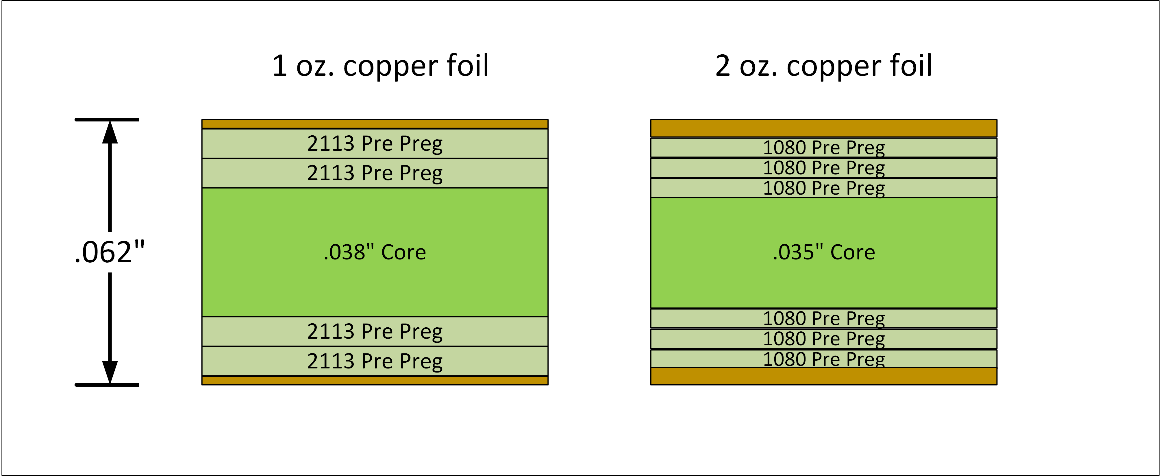
Providing you want to stay with the standard thicknesses, I’ll give you an example of PNC’s standard core thicknesses based off the core copper thickness. Let’s take an .062 and compare the stack-ups. See Figure  below:

Stack-up for an .062 multilayer:
062 thick PCB (002)


Notice to achieve the .062 overall thickness, the core thickness needs to be compensated based on the copper weight of the design. When using 1 oz copper we would use .038 core and .035 core for 2 oz. Also, the amount of pre preg would need to be adjusted as well to get to the thickness required. This is just one example when trying to determine overall thickness of your PCB.

The maximum PCB thickness is usually governed by something called the drill aspect ratio, which is the ratio of a drilled holes depth vs its diameter. When a hole is drilled, the deeper the holes becomes the harder it is to guide the drill accurately (because the drill deflects as it is pushed through the material) until you eventually reach a limit where you can no longer guarantee that the resulting drill hole will be centered in all the pads through the PCB. This is also referred to as drill wander in the PC Board fabrication world.

The aspect ratio for a through hole is the (board thickness) / (drill hole diameter).

Typically, the ratio is limited to approximately 10:1 This means that for a .062” thick board the smallest through-hole drill size is .006” which is the minimum drill size available at PNC. For a .093” thick PCB the smallest drill hole size will be .009” As board thickness increases, more complex via creation techniques such as laser drilled microvias are required to maintain the required pad density under components such as BGAs.

PCB thickness considerations for high speed circuits

One of the assumptions an electrical engineer makes when designing a circuit is that the PCB itself does not contribute any impedance to the circuit. However, in high-speed PCB design the integrity of the signals is definitely affected by the physical characteristics of the PCB.

Unfortunately for the designer the primary sources of parasitic capacitance and inductance of a PCB are affected by board thickness in conflicting ways, forcing the designer to carefully consider the trade-offs.

Vias

PCB vias can introduce both inductance and capacitance to the high-speed circuit. Parasitic inductance and capacitance of a via both increase proportional to board thickness.

Capacitance between layers
The capacitance between traces on different board layers or between traces and the ground plane are inversely proportional to the thickness of the dielectric between them. More space between layers will reduce parasitic capacitance and ensuring that all high-speed signal traces are the same distance from the ground plane will help impedance matching between them.

Crosstalk

Crosstalk between signal traces can be minimized by routing the PCB traces further apart and reducing the dielectric thickness between PCB trace and reference plane.

Mechanical Constraints

A PCB is ultimately a mechanical component of the product and is therefore subject to a variety of mechanical constraints. The PCB or PCBs must fit within the product envelope. This often requires that a PCB be as thin as possible. On the other hand, PCBs are subject to the torqueing forces from cables connected to the board edge and external connections. Preventing board failure during assembly or in use requires a circuit board fabrication thick enough to withstand these forces.

Finally, PCBs in the field are subjected to both vibration and shock. For example, large PCB panels can vibrate in several different modes when subjected to vehicle vibration, causing fatigue and eventual failure of solder joints. The rule of thumb is to get the resonance modes of a PCB to be 10X the input vibration. This requires designing thicker, stiffer PCBS and by careful placement and design of the PCB mounts.

These are the three most important considerations in selecting a PCB thickness. To optimize a PCB design, the PCB designer needs to understand all of these requirements and constrains on the PCB lamination stack-up, and have the flexibility to choose a PCB thickness that balances these often conflicting constraints. The team at PNC can help you design a PCB that meets your needs at a competitive cost and lead time.

Telescope

Ensuring a successful Turnkey PCB Assembly project

There are many detailed factors involved when pursuing the right company for your electronic or PCB assembly needs. These factors can be broken down into two distinct areas, customer communication and supplier contract review. Either the customer or the supplier cannot afford time lost if there is a misunderstanding or lack of data to efficiently and effectively produce a quality product on time. Time spent up front makes for a smooth and efficient transition through the quoting and manufacturing process.

Customer communication

A majority of communications for a request for quote, RFQ’s, in today’s industry are via email. The email needs to contain the required data files and be clear and concise in regard to quantities and delivery dates, along with any details that are not stated on the fabrication/assembly drawings. Since we are talking about Printed Circuit Board Assembly Turnkey projects, let’s break this down further with the required data files for PCB and PCBA.

PCB data files:

1- Fab drawing with build details such as material type, thickness, Copper weight, Tg rating, IPC-A-600 Class, Stack-up, Drill Chart, LPI & silk screen color, Serialization, Panelization array, MIL Spec, final finish and type(RoHs/Non RoHs) etc.
2- Complete set of gerber files.
3- Drill files.
4- IPC-356 Netlist for electrical testing.
5- Read me file for additional information not stated in fabrication drawing or email.

PCB Assembly data files:

1- BOM with manufacturers part number/description and alternates if applicable or DNP’s.
2- Assembly drawing with build details, Solder paste requirements, torque specs, IPC-A-610 Class, DNP’s, serialization, etc.
3- Pick & Place file.
4- ICT or Probe testing if applicable.
5- Functional test procedure if applicable.
6- Read me file additional information not stated in fabrication drawing or email.
If all the required information and data files are complete, we have successfully met the first half of the RFQ process. With this in mind, it’s up to us to compile this information in our contract review process. Let’s take a look at what is processed on our end to complete the RFQ cycle.

Supplier Contract review

All incoming turnkey projects are given an internal number for uniqueness especially for part numbers that has been revised. They are stored in a secure file folder based on two groups of data. ITAR data is stored separately than non-ITAR data. Once the customers data is stored and secure, engineering is notified to start to contract review process for the PCB and PCBA data sets.

Contract review for PCB:

1- Gerber files are imported and overlaid into correct layer structure.
2- Drill files are imported and overlaid against the gerbers.
3- If there is no IPC-356 Net list file, we extract the net from the gerber.
4- The gerbers are ran through a design rule check for manufacturability.
5- Fab drawing is reviewed by engineering for manufacturing capability.
6- If any discrepancies are determined, customer is notified immediately, If no discrepancies, engineering hands off the internal contract review check sheet to customer service.

Contract review for PCB Assembly:

1- BOM is scrubbed to ensure all parts are identified by manufacturer and P/N.
2- BOM parts stock research from approved vendor list.
3- Assembly drawing reviewed by engineering for assembly capability.
4- Pick & Place file review.
5- Review for testing if applicable.
6- If any discrepancies are determined, customer is notified immediately, If no discrepancies, engineering notifies customer service.
7- Quoting team is notified to officially create the quote and send to customer.
Customer communication and supplier contract review is a relatively simple step in order to achieve and ensure a successful assembly turnkey project. Adhering to the steps above can make for a great partnership.