Tag Archives: pc board assembly

Advantages of Laser Cut SMT Stencils for SMT Assembly

Laser Cut SMT Stencils:

Surface mount technology or SMT Stenciles is the procedure of mounting the electrical parts straightaway onto the PCB surface. SMT has replaced the through-hole technology technique of aligning parts with cable heads into holes in the PCB. The essential part of the SMT procedure is the covering of solder glue on the PCB. First, it is managed by screen impressing the solder glue with the assistance of solder stencils. Then, the solder glue is equally applied with the utilization of a squeegee.

Laser Cut SMT Stencils are laser-cut solder glue image stencils. It is organized for hand-operated solder glue impressing applications. These stencils are frameless, and it expeditiously eliminates the tiresome hand bonding of PCBs. Utilizing image stencils, you will be able to create your image on PCBs using your Gerber or CAD data file.

Five amazing properties of Laser Cut SMT Stencils:

  1. Laser-cut SMT stencils are created by utilizing the CAD data file that you provide. You can give a Gerber file for this as well. These data files are a two-dimensional graphic representation of every layer of a PC board where pads, vias, and tracks are presented with the assistance of different lines and figures. It depicts the electrical circuit board pictures, letting in the copper layers, legend; solder mask, drill information, and many more. These data files, either CAD or Gerber files, assists in producing the SMT image stencils for constructing a PCB board.
  1. Laser-cut SMT stencils typically bear a frame. Besides, it comprised of a sheet of stainless steel, in which the apertures are adequately organized. Utilizing it, they can squeegee the solder paste onto the PCB. Hence, it keeps the application of solder paste on amateur surfaces.
  1. The Laser cut SMT stencil generally is used on an full auto or semi auto screen printer using a squeegee blade. These blades traverse over the foil to deliver the potential paste volumes on the Printed Circuit Board surface.
  1. The laser-cut SMT stencils are usually stainless steel. It is utilized to assist the PCB operator in depositing glue or paste, onto the PCB surface. Steel stencils are more long-lasting and accurate than polyimide stencils. Often, other materials like mylar and nickel are used as well. Richly nickel substance stainless derivative has little grain, backing up better release attributes as the aperture surrounds are smoother. Precise release of solder paste through the aperture is essential. Additional solder paste deposition can make solder bridging. Lower solder deposition can make fragile solder joints that can involve the operation of the PCB.
  1. Laser-cut SMT stencils are laser-cut solder stencils. The laser-cut constructing technique improves the aperture definition and best dimensional leeways for more effective pitch apertures on the stencils. Hence, you will be able to have the best quality print with most minor faults. Laser-cut SMT stencils keep a precise and quotable solder deposition procedure. To utilize the laser-cut SMT stencils, set the PC board into the circuit board holder. Adjust the image stencil over the PCB SMT pads. Set the solder paste on the image stencil and disperse it through the whole width of the hole squeegee. Apply a squeegee to roll the solder paste over the image stencil coercing the solder paste through the image stencil on the PCB board surface.

 Advantages of Laser Cut SMT Stencils:

There are numerous advantages of Laser cut SMT stencils. Like:

  • Laser-cut SMT Stencils eradicates the mistakes that are expected to fall out in the hand soldering of image electrical circuit boards. The perfect laser-cut apertures enable fluent aperture sidewalls, hence bettering paste transfer. In addition, they are permitting post-processes of electropolish and nickel-metal plating to create the aperture walls articulate.
  • As laser-cut SMT Stencils are usually frameless, it reduces space requirements. Furthermore, it is significantly cheaper than framed image stencils.
  • These laser-cut SMT stencils are not glued in a frame, allowing optimal solder paste volume control.
  • Laser-cut SMT stencils can present fantabulous print performance and better the quality of your image Printed Circuit Boards.
  • Laser-cut SMT stencils are specifically organized to avoid the odds of whatsoever fault while using the solder paste on the PCB board. It also easy clean-up of the solder paste from the surface of the electrical board for quotable and precise solder paste deposition.
  • Laser-cut SMT stencils allow quick assembly with minimum cost. It brings down the PCB image assembly time. It is low-priced, concise, easy to handle, and easy to dispose of or recycle.
  • Laser-cut SMT stencils have a 24-hour turnaround standard.
  • Laser Cut SMT stencils have smooth inward pad walls, with geometrical fence changes of fewer than 3µm for best glue release features.
  • These stencils have aperture consistency for a decrease in expected defects.
  • These stencils have high pad positional conciseness for utmost good pitch accuracy in impressing. Tolerances of about 5um are possible with modern lasers.
  • Contrary to chemically engraved stencils, these stencils to Printed Circuit Board registration boast an exemplary circuit board to stencil registration.
  • These stencils have hyper delicate pitch designs less than 250µm can be recognized without problems letting you impress today’s challenging and outstanding pitch devices.
  • This stencil’s high accuracy of land visibility sound reflection in the stencil permits you to make an easy and authentic stencil position on PCB.
  • These stencil fabricating is performed straightaway from CAD/CAM data files eradicating problems with photo tool projecting and fictionalization quality and the caliber of surface planning and photoresist application to the queer as it is the same case with chemical engraving technique of stencil manufacturing.
  • These stencils bear chromium steel serving as ground material for these stencils has a high-potential rate. Hence, the stencil does not alter in size, and the aperture design is not disingenuous even after 10,000 impressing cycles that making the chromium steel stencil very authentic in usage.
  • Its smooth walls and pointed aperture profile. It was step-up the possibility of solder glue to pass over stencil apertures during every print cycle.
  • The laser-cut SMT stencils are easy to assemble and utilize.
  • These stencils create high-volume; chromium steel stencils are handy as they have a long span of life, allowing multiple utilizations for solder glue applications.
  • These same stencils permit you for on-contact and off-contact impressing on PCBs.
  • These laser-cut SMT stencils are efficient when utilized for multi-level impressing of PCBs.

How to check the size of the stencil?

The laser-cut SMT stencil size is compiled into 2 parts: inward size and general size. Inward size is the size well-matched, and that of PC Board set up to be collective, although overall size concerns the size well-matched with printer parametric quantity limit. As far as both sizings are precisely designed, the stencil will draw total usage of its functions.

Inward size of laser cut SMT stencil can be worked out adjusting to the following rule:

  • Width of Frameless stencil = width of PCB + 200mm while its Length = length of PCB + 200mm
  • Width of Framed Stencil = width of PCB + 100mm while its Length = length of PCB + 100mm

For instance, if one electric circuit board measure in size is 50*50mm, then the sizing of its bordered stencil should be about 150*150mm, and the sizing of its frameless stencil had better be about 250*250 mm.

It is comfy to remember and function, so it worked out for hand-operated solder glue printing in laser cut SMT stencils assembly before the coming of automatic printing machine. It can tell that different PCB sizings lead to propagations of different inward sizes of laser cut SMT stencils.

It derives from an automatic solder glue printing machine, all the same, relatively strong. The general size of these laser cut SMT stencil has to be ascertained by the parametric quantity limit of the printing equipment, that is, the printing machine, because stencil has to do work within the scope of printing machine with a frame. Diverse printing machines feature different parametric quantity rules. According to the conducted research, the stencil size congenial with our printing machine can be 650mm*650mm or 736mm*736mm.

PC Board designers have to focus on the internal size of the stencil; they don’t need to care about its overall size since it is generally determined by the parameters of the printer in your contract assembler workshop.

Final Words:

The laser-cut SMT stencils had better enable you to resolve your printing troubles to alleviate the PCB fabrication and assembly process. These stencils are well-suited for image fabrication, and the flapping helps keep the glue in an enclosed area during the impressing process. Furthermore, these stencils’ better accuracy saves time, and of course, step-ups yield. These laser-cut SMT Stencils are close-packed and easy to deal with. As an outcome, it has acquired popularity in offering faster and cost-efficient PCB prototyping.

These laser-cut SMT stencils that are decently designed enable highly effective PCBs that are uniform and quotable. This not just assists in saving up costs in the end, but it will also permit a higher-quality ultimate product. The team of highly competent technicians designs all the laser-cut SMT stencils with superior precision to assure you get the complete products that meet your requirements.

At PNC, you will get your design SMT Stencil’s requirements fulfilled at an affordable rate.

3D Automatic Optical Inspection (AOI) for PCB Assembly Introduction

The highest demand used in quality management of electronic printed circuit boards (PCBs) and PCB assembly is automatic optical inspections and automated optical inspections (in short, AOI) (PCBA). AOI inspects the electronic assemblies such as PCBs mechanical visual inspection to ensure that the components of PCBs are in the right place and the contacts are correct.

Automated optical inspection (AOI) is an intelligent visual inspection of the production of the printed circuit board, where all catastrophic failures (such as broken components) and quality faults can be scanned automatically by a sensor.

It is widely used in the production phase because it is a way of testing without touch. It ensures the multi-layer circuit boards provide a high degree of durability.

For the following various applications, it is essential:

  • Infringements of line spacing
  • Violation of spacing
  • Copper excess
  • The shortage of pad
  • Short circuits
  • high frequency
PC board
PC board

What does AOI inspect?

AOI is a primary method used to build and test electronic printed circuit boards and PCBs for automatic or automatic optical inspection. Automated optical inspection, AOI allows quick and precise assessment of electronic assemblies and, especially, pcb assembly to ensure that the standard of goods is good and that the object is appropriately and without processing defects.

What is the need for AOI inspection?

Current circuits are much more complex than boards were a few years back, notwithstanding the significant changes that have been developed. With the advent of surface mounting technologies and more size decreases, boards are exceptionally lightweight. Even comparatively ordinary panels have millions of fused joints, and most issues are observed.

This growth in board difficulty also implies that manual examination is currently not a feasible choice. Even if the solution was approved, the inspectors quickly fatigued it, and poor and wrong design was easily overlooked. With great demand, high-quality goods on the market now require very simple, very stable, and fast.

To ensure that the product quality continues to be good, methods are required. AOI is an indispensable instrument within the context of an advanced electronic test plan, ensuring that the expense is held to the lowest possible levels by identifying faults at an early stage of manufacturing.

Benefits over manual visual inspection

PCB devices switch to ultra-thin, lightweight, higher densities, and exemplary size components. The part assembly width of the circuit board has increased, the width and distance of the Printed Circuit Board -line and the pad are decreasing and reaching the micro-level. The manual process of visual examination cannot be achieved. Furthermore, people seem to be tired and emotionally affected, according to the textbook. Inspection equipment is more stable, repeatable, and precise when it comes to machine vision.

Manual visual examination is a vital part of our BES operation. All new boards, either we order from a new supplier or a well-experienced BES company, are visually inspected by us. From solder masks to solder joints, we test all on the floor. Shipping packaging is also evaluated. When we develop our projects, manual visual testing is also helpful throughout the development, from designing to large-scale production. It was the first phase in our identification and repetition of design or manufacturing problems.

  • The usual general information SMT operator will fit well for quick and easy manual visual inspection.
  • Manual visual inspection with high flexibility;
  • The original costs are minimal, and only the initial Labour costs are spent, and high expenses are not available;
  • Preparation is fast.

How can time save done from the visual inspection process?

Visual inspection proves to be a game-changer, with many apps in almost every domain. The company is now moving into manufacturing and production, enabling them to use the power of profound learning and thus have quicker, safer, and superior automation.

  • More quickly

CPU speeds, as calculated in FLOPs and even accurate measurements, result in observations and conclusions, which are done incredibly quickly.

  •  Accurate

An automated machine can standardize the measurement of absolute measurements.

  • Trustworthy

The machine is impartial and programmable as required and without doubt following instructions. It is undoubtedly a result of this technological transition that is moving global producers into different production and productivity levels.

Final Thoughts

AOI is a vital factor in ensuring the accuracy of your completed electronics items is defective and accurate. It gives a shorter timeframe, more efficiencies, and lower prices, which would have increased if reworking was required.

The AOI process provides reliable monitoring and resulting information which enables improved quality control procedures management and the correction of potential issues. The algorithms will monitor the successful and defective PC Board components and record them. Efficiency is also improved from the point of view of process control, organizational integrity, and reporting.

The controls provide search, identification, and measurements or diagnosis for the outgoing product condition. Inspection is an operation. Tasks of supervision have typically been assigned to people. Efforts to simplify industrial inspections to eliminate mistakes and reduce monotony have encountered technical constraints and cost factors of deployment. A prototyping model is an occasional compromise. Reviews have released new study status on manual, hybrid, and automatic inspection.

Perhaps the most critical inspection process is the visual inspection of the parts made. Draw the section and equate the area with the painting visually. For units with several functions, this is particularly relevant. Anything may go wrong, and one of the several production cycles.

During AOI, optical inspection algorithms usually use visual techniques to ensure defects on written platforms. They can identify a range of material removals, such as nodules, scratches, and marks, as well as known dimension faults, such as open circuits, shorts, and solder integrity. They will also spot faulty components, missing components, and parts that have been misplaced. All system is designed to monitor tests conducted by manual operators can be carried out much quicker and more reliably.

How can We (PNC ONLINE) help you in 3D Automatic Optical Inspection?

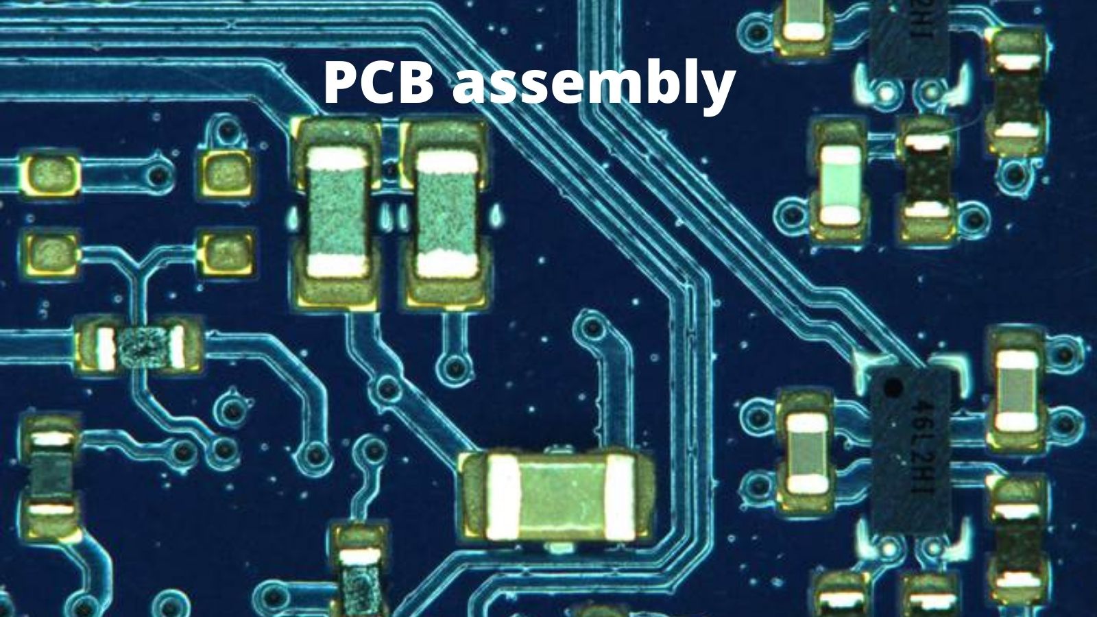
At PNC, you will get your design checked from two (2) Mirtec MV-6 OMNI machines which itself is high-speed/high-performance 3D AOI MACHINE FIFTEEN MEGAPIXEL CoaXPress Camera Technology. It has an advanced eight-phase Color Lighting System Ten Micron / Pixel Precision Telecentric Compound Lens. It is designed with an Integrated Ten Mega Pixel SIDE-VIEWER® Camera System Precision Closed Loop AC Servo Drive Motor System which is extremely simple to program and operate. It also has 3D Co-Planarity Inspection – Gull Wing Device with an example as shown below:

PCB Assembly
PCB Assembly

We follow all the system parameters and are set up to meet IPC inspection requirements. Get your Automatic Optical Inspection done for your 3D design at PNC. Contact us at sales@pnconline.com


Work with PNC to Reduce PC Board Costs

When it comes to reducing the manufacturing cost of a PCB, it is important to remember that a significant part of the cost of a PCB assembly is already baked in at the design concept stage.  The product concept defines the PCB size and shape, while the performance of the system dictates the microprocessor, memory and other functional elements of the circuit.

However, some of the assembly cost can still be affected by design choices made by the PCB designer.  A PCB that is designed for manufacturing (DFM) can reduce both the fabrication cost of the PCB and the costs of component assembly and soldering. A DFM approach to design can also reduce the likelihood of the hidden costs of poor yield in production.

The best way to achieve the lowest cost, most manufacturable design is to work closely with the prospective  manufacturer, since the way to maximize DFM cost savings is to design for a manufacturer’s specific equipment and technology, rather than to rely on general rules.

Reducing PCB Fabrication Costs

The first step to reducing costs in PCB fabrication to reduce the number of operations performed by the manufacturer.  The second step is to optimize the PCB design to leverage a manufacturer’s particular fabrication technology.

One way to reduce costs is to eliminate or minimize the amount of machining required around the board edge or within the PCB itself.  Rectilinear PCB outlines without internal slots will minimize machining, and the rectangular shape allows the PCB to be grouped in larger panels that are separated after assembly.  These large panels streamline assembly by allowing a several PCB to go through component assembly and reflow at the same time, improving throughput. For example, PNC can process a maximum panel size of 18” X 24.” To ensure that the components on the PCB are not damaged during the scoring and separation from the panel, components should be kept 200 mil from the board edge.

Reducing board layers to reduce fabrication costs

The generally accepted rule that reducing the number of PCB layers in a stack-up will reduce cost has become more complicated with the advent of HDI technology.   The reason is that the cost of an additional Printed Circuit Board layer is not linear, so a cost calculation needs to be made for each jump in the number of layers. Is it cheaper to use finer trace widths and buried vias to reduce the layer count from six to four?  Only the manufacturer is going to know.  However, as a board gets past eight layers costs increase non-linearly with each additional layer.  The aspect ratio of the through hole vias begin to become a factor, as well as the sheer number of vias that need to be drilled and plated to connect all those layers.   At an eight layer stack up or above, the additional cost of HDI technology begins to make economic sense if it is used to reduce the number of stack-up layers required.

Respect drill to copper clearance and aspect ratio design rules

Respect the design rules for hole sizes and hole to copper clearance.  If the real estate on the PCB allows it, selecting hole sizes clearances and annular ring sizes larger than the absolute minimum will improve fabrication yield. Here are the through hole design rules for PNC:

Non-Plated Through Hole (NPTH)
● Finished hole size (minimum)= 0.006″
● Edge to edge clearance (from any other surface element) (minimum)= 0.005″
Plated Through Hole (PTH)
● Finished hole size (Minimum) = 0.004″
● Annular ring size (Minimum)= 0.004”
● Edge to edge clearance (from any other surface element) (minimum) = 0.009″

PCB assembly
PCB assembly

Reducing PCB Assembly Costs

To reduce assembly costs the objective is the same as reducing PCB fabrication costs; reduce the number of operations, and optimize the PCB design to leverage a manufacturer’s particular fabrication technology.

One easy way to reduce assembly costs is to stay away from the smallest passive packages.  0603 passives are easier to place than 0402 or the almost invisible 0201.  If possible, chose active parts that have leads rather than ball grids, because they are easier to place, they can be visually inspected instead of x-rayed, and they are easier to rework.

Avoid parts that have to be manually soldered.

Manual operations are always expensive, and the designer should do everything they can to avoid the need for them.

Component manufacturers have recognized this and now offer through-hole components (typically connectors) that can be reflow soldered.  This technology called “Through-Hole Reflow” allows through-hole components to be soldered in the same reflow process as the SMD components, eliminating a pass through the wave soldering machine or manual soldering.

Finally, if possible, avoid putting components on both sides of the board.  The cost of a higher density PCB with components on one side may be cheaper than a lower density PCB with components on both sides.

Don’t wait until the PCB design is finished before talking with PNC

The best time to talk with the PC Board design experts at PNC is early in the layout process.  They can tell you when to use HDI to reduce costs and can advise on how to optimize panel size. The experts in the assembly department can also work with you to select components that will reduce assembly costs and increase yield.

Give PNC a call today.

Embedded software development along with PCB Assembly

No company can excel at every aspect of new product development and trying to do everything can dilute an organization’s focus on the tasks that are essential to its success. For example, most companies have long ago outsourced the PCB design and fabrication steps of new product development. This same need to focus on the essential is true of software development too. It is difficult for a software company to excel at every type of software development because of the ever expanding universe of software languages, operating systems, and architectures.  A cloud based SAAS or PC based application is very different from embedded software running C on a 16-bit processor, and it takes very different software development skills to develop that kind of embedded application.

Unlike cloud based or PC based applications, embedded software is optimized to run on a specific custom hardware platform with limited processing power and memory.  It often runs on a real time operating system or no operating systems at all, and the interface of an embedded device may consist of only a small display, or just a few buttons and LEDs.

The unique challenges working with embedded systems is why many software companies outsource their embedded software projects to experts like PNC.  Here are three reasons why they do.

The embedded system is not the organization’s primary product line.

Many products on the market require options or accessories that are important to the customer, but not are not similar technically to the primary product. A cable set top box remote is a good example.  Customers expect a cable set-top box to have a remote, but the low power microcontroller embedded in the remote is likely to be completely different from the high power processor and OS driving the set-top box functions.  Similarly, Industrial or commercial equipment may have optional modules to provide additional functionality like a cellular modem.   These optional modules have independent processors and embedded software which is unrelated to the primary product software.

In these cases, software companies will choose to focus their development resources on the primary product, recognizing that it is more cost effective to outsource the software development for the ancillary embedded products to a company that is familiar with embedded microcontrollers and the constraints that come with low power operation. If that company can design the hardware and perform SMT assembly too, it becomes an even better value.

Embedded software development along with PCB Assembly

The software is deeply embedded and invisible to the user

Successful software companies are highly focused on the customer experience with their product. They are constantly refining the look and feel of the industrial design and user interface to make the product more attractive, and easier to use.  But what if the product doesn’t have a user interface?   What if it is a router or a motor controller?  Products like these need a simple interface for initial configuration, but they typically operate in the background, invisible to the customer.  In this case the goal is to optimize for cost and performance rather than user experience.  Deeply embedded applications without a sophisticated customer facing interface  are ideal to outsource to a company like PNC because the product requirements are centered on the embedded functionality – there is no need to maintain the same look and feel as the company’s customer facing products.

The application requires specialized expertise

 Sometimes a software company needs embedded expertise that it just doesn’t have in-house.  For example, they may need a Zigbee or Bluetooth RF stack, or expertise with digital signal processing on low power Digital Signal Processors DSP.  In some challenging embedded applications, a company may need a partner with the expertise to  iterate the design of both the hardware and software simultaneously to arrive at an optimized embedded solution.  In that case you need a full service provider like PNC.

PNC offers the full solution to developing embedded products

When it comes to product development, PNC is not just a PCB manufacturer.  The engineers at PNC can work with you to design and manufacture the product hardware, and then develop the embedded software to run on that hardware.   If you have a challenging embedded software or hardware project, contact PNC today and find out how they can help.

PCB assembly Pre-Reflow FAI

First article inspection (FAI) prior to SMT assembly is a design verification methodology that provides a reported verification and validation of details of a product on the shopfloor per its manufacturing procedure and requirements. There are various ways to perform FAI, from both supplier’s and customer’s side, making it a very dynamic process. This means that each organization can tailor its FAI method to benefit itself and consequently, its customer, yet maintain rigid performance standards at the same time. FAI involves qualitative and quantitative measurement. FAI is also highly effective since it can potentially fulfill process validation requirements of quality management systems like ISO9001 or AS9100.

In the PCBA manufacturing industry, FAI can be effectively employed in validating materials for manufacture, underlying technologies, manufacturing processes used, packaging, and equipment. It can also be applied to a batch of a given sample-size from a mass-production instead of just the first sample, as the name might suggest. At PNC, strict adherence to our manufacturing standards helps in production with better yield but at the same time, facilitating dynamic validation techniques in our manufacturing process allows us to reduce lead time. The focus of FAI in PNC assembly lies in validating the pcb assembly before reflowing so that the SMT team can make necessary adjustments for the next batch, saving time and effort during rework. They are also responsible for validating the correct loading of the right component in its allotted slot per the assembly program. This extra step helps in validating the placements of the components and improves the turnout rate for a successful production.

All aspects of reflow also must be amenable to improve solder performance and the same translates to our guideline where only the most recent batch of solder paste (with most activity) is permitted for use, which is validated by FAI. Apart from pre-reflow FAI, post-reflow X-Ray also helps validate the solder performance based on the reflow profile which can then be adjusted accordingly so that all components are successfully soldered. This can be similarly implemented at the rest of the printed circuit board assembly stages as well up to testing. But there is a necessity to establish a constant groundwork or point of reference in such a dynamic process to give each validation at a particular stage, the perspective of what changes were made before. This is achieved by using a single piece of documentation used to validate at every stage, wherever applicable, and that document reports any changes made to the processes or product, to the next stage.

pcb_assembly
pcb_assembly

PNC employs the use of AEGIS software to combine SMT assembly guidelines and inspection requirements into a single document (internally referred to as AEGIS). The AEGIS is used to report every single FAI validation to different stages of assembly. PNC’s FAI process for SMT starts with thorough solder paste FAI & its validation, which will be detailed in another post. For this post, let us consider pre-reflow FAI and highlight its validation process since it is the most crucial stage. The procedure is as follows:
1. The SMT team confirms the correct allocation of components as given in the assembly program. This is done by comparing each component with its description, measuring component value wherever applicable, and checking for physical marking on ICs. This helps in validating that the right component has been placed in its respective position on the board.
2. The next step involves checking for the polarity of components, wherever applicable. This is a two-step process. First, the supply angle of a component in the reel needs to be checked and second, the placement of that very component on the PCB needs to be verified.
3. Now, once the first board is assembled, the pcb assembly is put through FAI, where the placements of all components on the board are checked, any necessary placements that remain are placed manually and polarities of applicable components are checked and changed as per what is given in the AEGIS. The same changes are made in the assembly program to avoid the same occurrence in the rest of the batch. Components that are designated as DNP (Do Not Place) are also checked and finally, the solder paste information such as solder type, lot number, date of manufacture, and expiry are checked to ensure that the right solder paste has been used.
4. All these checks translate to notes, remarks, and checks on the AEGIS document, which can then be referred at later stages up to final inspection. If the job in consideration is a repeat job, it can be optimized to avoid any errors made in the first batch of production.
5. The board is then sent through reflow. Once reflowed, the board is extensively inspected under high magnification camera for quality of component placement, solder joints etc. yielded by SMT process.
6. Each section in the AEGIS is meant for FAI by a different team performing a different operation.

PNC has been able to reduce its lead time and increase customer satisfaction significantly and our personalized and successful FAI is a big factor contributing towards it. Further development to the FAI process is underway as much as it is needed to achieve better production yield over time for all the different types of PC Board assembly that are assembled at PNC.