Tag Archives: printed circuit assembly

What is High TG In PC Board Fabrication?

The making of PCB involves different steps, technologies, and terms, and TG is one such term that refers to the Glass Transition Temperature. High TG PCB is the board made at a high temperature. We will discuss this topic in detail, including the TG value, features, applications, materials, parameters, and much more.

What is High TG PCB?

If a PCB’s temperature goes beyond a set TG value, its condition will change. Like, the solid board will turn rubbery, affecting a PCB’s function. Depending on where you use a PCB, the temperature of the application should be at least 10 to 20C less than the PCB temperature.

Understanding TG Value

TG means Glass Transition Temperature like there is a certain limit of this temperature for PCB and that specific temperature is the TG value. TG value helps in understanding the PCB material, and you can find which temperature is required for its service.

Secondly, it helps you to find the condition of the PCB material, like if it’s solid, flexible, or solid-flex.

High TG PCB and Its Features

You have to choose a high TG Printed Circuit Board for your application carefully, because it involves multiple features, including thermal, electrical, mechanical, and chemical features.

Thermal Features: they include the TG or Glass Transition Temperature, thermal conductivity, thermal temperature’s coefficient, and decomposition temperature. TG is the temperature at which the state of the PCB material changes. But, when the board cools down, it gets back to its initial condition.

Electrical Features: they include the surface resistance, electrical power, volume relativity, and the dielectric constant and loss tangent.

Chemical Features: the chemical properties of a high TG PCB include the moisture absorption and the methylene chloride resistance of the PCB material. The TG PCB should be able to resist moisture if it’s near water.
Mechanical Features: the mechanical features are also important to know regarding the TG PCB. They include the flexural and peel strength, and the young’s module.

Suitable Materials for High TG PCB

A PCB has two materials, including laminate and substrate. The substrate includes epoxy resin, glass, or paper weave. The substrate should be compatible with the TG. Some common substrates that we use for a high TG PCB are;

  • CEM-1, 2, 3,4, and CEM-5
  • G-10 and 11, FR-1 to FR-6
  • Aluminum
  • Knapton
  • Pyralux

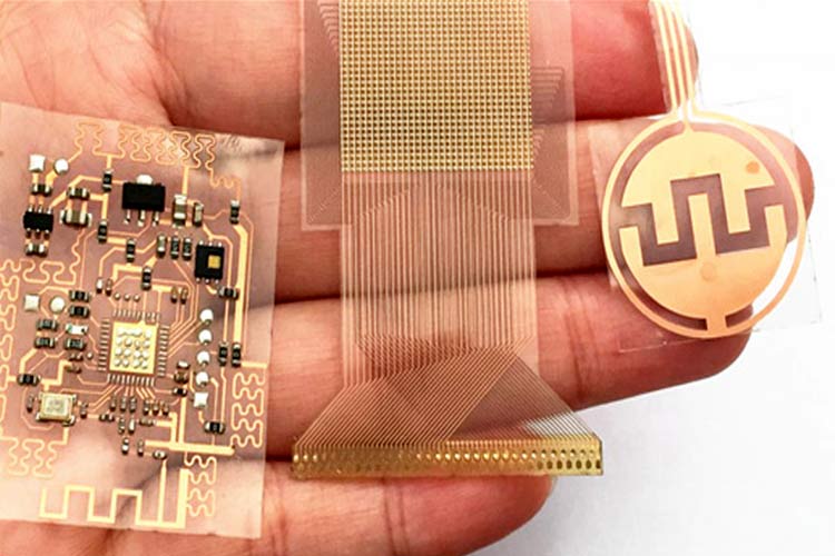
The last three materials are flexible.

The laminates should also be compatible with your TG PCB in terms of strength and temperature. Some common laminates are:

  • FR-1, and FR-4
  • CEM-1, CCEM-3
  • Teflon

Criteria for High TG PCBs

Printed circuit boards with a high TG value are based on certain criteria as described below:

  • The selection of a PCB, depending on the components like it can be single or double-sided PCB or embedded.
  • The stack-up PCB with a single layer or several layers
  • The design of such boards can be based on a module or it can be custom
  • The strength of the board also matters, like it should be robust either electrically or mechanically
  • PCB’s bendability also helps to classify the TG PCB, like if it’s hard, flexible, or hard-flexible
  • The electrical strength also helps classify the TG PC Board

Generally, manufacturers use bendability and strength to classify a TG PCB‘s physical properties.

Where Can You Use The High TG PCBs?

You can use the high TG circuit boards in intense conditions, as the environments with high-vibration devices. They are also suitable for applications with shocks, chemical components, and high temperatures. Like, missiles and car parts often come up with chemicals. So, the suitable industries for high TG PCBs include aerospace, telecommunications, military and defense force, automobile, and down-hole drilling.

What to Consider While Designing a Rigid PCB?

You must hire a professional PCB manufacturer for the right design, manufacturing, and assembly of these boards. The engineer must know the kind of environment that suits a TG PCB to function precisely. Below are a few examples to help you understand it.

Commercial Use

Many telecommunication companies use the best materials for mobile devices to enable them to bear high shocks. Like, the phone should not get damaged easily when you drop it.

Auto Industry

PCB has to be safe under a car’s hood as it’s mostly vibrating, so a shock or crash might happen. Hence, a rigid PCB is the best solution in this case.

Aerospace Industry

The flying machinery always needs the high TG PCB because there is intense vibration, like in the jet engine, as there are thousands and millions of micro-vibrations in one minute. So, equipment related to aerospace should be able to tolerate extreme temperatures, like from -45°C to 85°C.

Other Applications

These boards are also ideal for solar power equipment, such as power inverters and cogeneration equipment. As these boards resist temperature, they work well in many industries. Like, one of its applications involves Lead technology, like the medical, computer, and telecommunication industries.

The TG PCB is also used in broadcasting, like booster stations. Besides, the fire detectors and burglar alarms also need such boards.

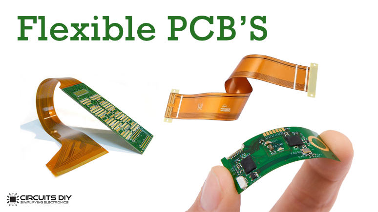
Use of High TG Flex PCB

It is clear from the name that a flex PCB can adapt any design or shape to get compatible with certain products. Like, they can tolerate intense environments better than rigid PCBs. You can use the high TG flex PCB in defense and military, aerospace, medical equipment, consumer electronics, auto, wireless networks, as well as industrial equipment.

What To Consider While Designing a Flex PCB?

You must hire a professional PCB manufacturer for the right design, manufacturing, and assembly of flex PCB. The engineer must know the kind of environment that suits a TG PCB to function precisely. You should see if:

  • You need a flex PCB for an ordinary environment or an extreme environment like an explosion. Whereas the cell phone has a normal environment.
  • The environment should be free from any moisture before installing a high TG circuit board.
The Design Process

The design of a high TG PCB involves different steps, such as

  • Using the right software, like CAD, Eagle, Altium Designer, etc.
  • You must know the power requirements to suit different components on the PCB. You should also consider a specific plan for noise reduction caused by a TG PCB.
  • Preparation of the stack-up plans documents as it is essential for making the best TG PCB.
  • The floor layout for a PCB with proper sections, including components. Like you can place them together or separately.
  • TG PCB should be complete in terms of a power plane and ground details. These details ensure proper routing for signals.
  • The board should be compatible with patterns in terms of sizes. All components should be well-placed to help a PCB function the right way.
  • It is important to design routs for high-frequency signals, as the route should be clear for a flawless signal transfer. This step involves vias, as they help in proper signals. You need the reverse via and signal via in this case.
  • You must follow the 3W-rule to increase the traces’ distance which helps to reduce the coupling effect.
  • Another rule to reduce the coupling effect is the 20 H rule.
  • In the end, check the routing guidelines to see if you are doing everything the right way.
Specs and Design Parameters

The fabrication of a high TG PC Board Fabrication involves certain parameters and specs, depending on the application. Some standard parameters are described below.

How Many Layers Do You Need

Designers prefer the even number of layers while developing the high TG PCBs. But, the odd numbers of layers are also suitable in certain applications.

Dimensions of PCB

The PCB dimensions depend on its application. Like, you need a large circuit board for a broader application. Besides, there should be enough space on the board to place the electrical components.

Well-Finished

The high TG PCB should be well-finished, and the material depends on where you want to use this board. Like, some common materials are;
HASL, or hot air leveling – It is ideal as it is cheap and can be stored for longer.
OSP, or organic protective surface
Immersion silver – It gives a smooth surface, and it is cost-effective. It has many storage limitations
Immersion tin – It suits the SMT

Immersion gold – It can be stored for longer with a few limitations.

ENEPIG, nickel palladium – It can be stored longer, but it involves a complex process.

Solder mask – It protects the PCB from environmental elements.

Weight of copper – You must also consider the weight of copper like it includes both initial and finishing copper. Generally, the weight is 1 oz. to 1.5 oz. or 5 oz. It also depends on the layer and board thickness.

Assembled PCB thickness – The TG PCB thickness depends on its material and type. Like, if it’s flexible, hard, or a hard-flex board.

Distance between layers – The distance or spacing of electrical components and layers should be equal for high-frequency signals. As it reduces the coupling effect.

Via sizes – The drill aspect ratio and the hole size should also be appropriate. Generally, the PG PCB can have either plated-through or non-plated through holes, depending on the placement and layout design.

Board quality – The board should have a high-grade material to ensure an effective function during application. Besides, you must check the quality of the TG PCB to evaluate its performance in terms of specs. Like, you should test its lamination, vias, copper plating, solderability, finishing, components, and cleanliness.

Interested to know more about PCB TG or PCB Assembly? Email us at sales@pnconline.com

10 Most Commonly Used Components in PCB Assembly

10 Most Commonly Used Components in PCB Assembly

How many times in a day do you generally catch yourself using an electronic gadget? Maybe a hundred times like right now. Although we are living with these electronic gadgets, understanding the mystery behind the electronics is still a mystery that needs to be resolved. It is not that difficult to understand the basic functionality and structure of every electronic device.

The reason is almost every electronic device tends to have some similar basic elements in its infrastructure. But still, it seems difficult to understand the working of the electronic device because nothing is happening in front of the eyes visually. Despite all of the facts, it is still interesting to read and understand about electronics. Moreover, it is not unthinkable to start building various electronics projects with a little background knowledge.

Now, let’s move to the very basic and essential part of the electronic industry, and let’s discuss its details so we can understand it well. And that basic thing is the printed circuit board (PCB).

What is a PCB?

Have you ever seen a building? What is it made of? Blocks of bricks, right? Similarly, an electronic device is made up of blocks known as printed circuit boards. The main advantage of a printed circuit board is that it helps in connecting the various components of electronic devices to build a cohesive system that offers power to different devices.

Just like a building designed as top floors, ground floors, rooms, balconies, printed circuit boards are designed to make a connection between different parts of the building (electronic device). And this connection then provides a fully functional electronic system that is capable of providing power to the other devices.

For the past couple of years, printed circuit boards have been used in various electronic devices to improve their functionality and quality. Moreover, these circuit boards make the device more reliable and easier to use. Depending on the type of device, a printed circuit board can be single layer to multiple layers. Generally, multilayer printed circuit boards are used for complex devices. Multiple layers circuit boards also have complex structures. Now let’s understand the structure of printed circuit boards.

What are the components of a PC board?

As we have discussed before, printed circuit boards are the building blocks of any electronic device. That’s why they are made up of different electronic components depending on the functionality of the device they will belong to. These components play a smooth role in the better functionality of the device. If any of the components fail, the entire system would fail and as result, the quality of the product would be affected. So effective functionality from each component is required for better working of the device.
Following are the commonly used components in a printed circuit board. The components mentioned below are just for beginners because as we have mentioned before, the multilayer circuit board will have a complex structure. Mostly used components in a printed circuit board are discussed below:

Capacitor:
As you already know that capacitors are used when we need to store electrical energy. Capacitors are essential for storing energy and you will find it on every printed circuit board. A range of electric charges is stored in a capacitor, and they act like storage space or a battery for the circuit board. The capacitor can gain and lose full charge that’s why they are used in the filter process. In this process, an electric device can use the backup source of energy if it loses the main source so that it does not lose the data. Capacitors release the energy when the device needs power. There are various types of capacitors available such as ceramic capacitors, polyester capacitors, and radial capacitors. The categorization of the capacitor is done on the basis of the insulating material used in them.

Resistors:
Resistors are commonly considered the first and essential part of any circuit board. They are used to control energy flow with the device. They are also referred to as the foundation of current control. Electric current is transmitted, and heat is dissipated in the resistors. They provide ease to the electric flow in the electronic devices. The level of resistance of the object can be defined by analyzing its resistance. The flow of electrical energy is resisted to form heat and what is then dissipated. There is a wide variety of resistors. The recommended resistors for the beginner are made of carbon film. The different colors in the body of the resistors show the resistance value.

Inductors:
Inductors are also used to store energy. So, we can say that they are similar to capacitors in nature. The energy is stored in the form of a magnetic field. This magnetic field is generated with the flow of electric current within the device. Moreover, inductors are also used when we need to block some signals. For example, interfering with the flow of signals from another device.

Transformers:
As clear from anime, transformers are used to transform energy from one power source to another. The induction process is used for this purpose. Similarly, transformers are used in printed circuit boards for transforming energy. The electrical is transferred from different circuits and then converted according to the need by increasing or decreasing the voltage. This function is somehow the same as the resistor as it regulates the current. But transforming current provides more electric isolation than a normal resistor. There are two windings (soft inductive circuits) and an iron core in the transformer. Both winding act as sender and receiver accordingly. The primary winding is the source of the energy, and the secondary winding is where the energy will go. The large voltage of energy is broken down into smaller parts by transforming so that the device or the equipment would not be overloaded. This helps in achieving the manageable flow of the electric charges in the circuit.

Diodes:
A Diode works in the same manner as the resistors. Electrical resistance is used to control the flow of the current. They assign a specific way for the high and low resistance. The hi8gh resistance is offered on one side and zero resistance on the other side. In this way, electrical current can be managed from flowing in the wrong direction. Because the wrong direction of the flow can also damage the functionality of the device and the equipment. The most common type of diode that you may have seen is light-emitting diodes (LEDs). Moreover, Zinner, high-speed switching diodes are also available and used for different purposes.

Transistors:
Transistors are used to amplify energy. Transistors are fundamental to all the new electronics. Their role is vital and sometimes they are referred to as the building blocks of the electronic device. A commonly used transistor known as a bipolar transistor can amplify current in three different directions as it has three areas and three pins. Bipolar transistors are further categorized into NPN and PNP types. Both types are made up of base, collector, and emitter. The switching and controlling of the electric current in the circuit are done by the transistors.

ICs (Integrated Circuits):
As clear from the name, integrated circuits are smaller circuits that are placed in the printed circuit board by minimizing the size. They are made up of silicon and then covered with plastic. The calculation is performed by using analog technology in modern integrated circuits. Integrated circuits are the source of energy for printed circuit boards. They provide power consistently that’s why they are also called the powerhouse of the PC Board. Transistors, resistors, and capacitors are collected in ICs as they can oscillate, amplify and process the energy within the circuit.

Batteries:
As it is clear from the name, batteries are used as a source of power in the PCBA. This is probably the most purchased component for the printed circuit board and is generally used by non-electrical people as well. The main function of the battery in the printed circuit board is to convert chemical energy into electrical energy so that power can be provided to different components of the board. An external circuit is used by them for the flow of electrons from one electrode to another.

Sensors:
Sensors are used when we need to analyze the change. They sense the change in the environment. The electrical signal is generated according to the change that has been detected. The signal is then sent to other components of the board.

Switches:
Switches are the power buttons of the printed circuit board and are used by non-engineers, the same as batteries. Switches are used for a variety of purposes but in pcb assembly, their function is to control the flow of the current. The flow can be managed by opening and closing the circuit. Push-button switches, toggle switches, and micro switches are commonly used types for the circuit board.

PNC is the leading brand in terms of providing a turnkey solution for all your PCB-related requirements. Interested in pcb assembly services? Just write us at sales@pnconline.com

What is the BGA of PCB Assembly

What is the BGA of PCB Assembly?

What is BGA (ball grid array)?

Ball grid array (BGA) is used in integrated circuits for circuit mount packaging. Ball grid arrays are used when we need to mount the devices permanently such as mini processors. The connections are made on the bottom of the SMD ball grid arrays. A solder ball is present on every single pin. A uniform circuit for the grid is also made on the circuit for better connection. The size of this grid varies from 1.27mm to 1.0mm. Although there are hundreds and thousands of component connections present on each layer, the number of routable pins per layer is limited. The via and the routed connection should be applied to the inner pion of the layer as this technique is known as DogBone. There is another technique known as via in pad which is used when the circuit needs the pads in the solder masking and the pitch of the circuit is relatively small. Ball grid array is recommended because it provides more interconnection pins. The solder ball is also provided with every pin.

These pins can be put in flat, dual, and inline packages. The distribution of connection on the even and uniform circuit is compulsory. The bottom perimeter is also used sometimes but the whole button surface is more preferred. The process of the ball grid array is critical and needs to be done carefully while following the instructions. Soldering in a ball grid array is done in an automated process and needs complete control over the process. That’s the reason the ball grid array is not recommended for socket mounting.

The thing that needs to be noticed in the ball grid array is there is no direct lead that connects the ball grid with the circuit. Instead of leads, the ball grid uses solder balls to make a connection with the circuit and to pass the electric current. There is a physical connection made between the substrate and these balls during the smt assembly process. The physical structure is connected to the substrate by a wire which is responsible for the flow of the current. The conductive traces present in the trace are responsible for sending electric signals. This flow happens between the bonds and the substrate and the base of the balls.

There is a term known as ball grid re-balling. This technique allows the reusability of the component. That’s the reason it is most recommended. The scrapping rate is low in rebelling. This process is cost-effective and time-friendly because the ball grid package can be removed. This also saves the material of the entire process. In fact, the cost can be decreased in a high ratio if one selects to reuse on a ball grid array.

Why choose a ball grid array for PCB?

Ball grid arrays are used in printed circuit board packaging because of less density and low cost. Undersize chips are used for the interconnection of the circuit. On the other hand, there is another chip known as a conventional chip in contrast which uses the perimeter section for the interconnection. The printed circuit board has relatively high performance and more space for connection.

Moreover, the thermal resistance of the printed circuit board is low. It offers high performance at high speed. Printed circuit boards made from this technique are more reliable.

Types of ball grid array:

There are three types of ball grid arrays. These types are mentioned below:
• Ceramic ball grid array (CBGA)
• Plastic ball grid array (PBGA)
• Tape ball grid array (TBGA)
Each type is crucial in the processing and making connections and each part has its detriments. The selection of the right solder is important for better performance. That’s why relative types should be chosen for certain work.
Let’s understand the functionality of each type in detail.

Ceramic ball grid array (CBGA)
This ceramic package is used when the substrate used is of ceramic type. There are many further types of packages that come under the umbrella of ceramic grid arrays. For example, CCFA and LGA. The ceramic material is used when the temperature rate is high as the base material is ceramic. These types of chips are used in computer mini processors. Multiple layer packages are used in this type. The flip-chip method is preferred over the wire bond for the interconnection of the die. The reliability of the ceramic grid is increased by adding ninety percent lead with tin in ten percent quantity.

The difference in thermal coefficient of expansion in the substrate is also controlled by using this method. The packaging density and heat dissipation is high in this type. But the manufacturers have to compromise over the thermal compatibility as it is quite low for a printed circuit board. Moreover, the ceramic process makes the cost higher. So, this is not a cost-friendly type.

Plastic ball grid array (PBGA):
As clear from the name, the base material for the body package is plastic in this type of ball grid. It offers high density and solves the cost issues by combining the over-molded pas array carrier and glob to pad array carrier. Sixty-three percent of tin and thirty percent of eutectic tin is combined in the solder balls. The substrate is made in the sense that it can deal with at least 150 degrees Celsius of temperature.

The size of the normal package of the plastic grid is almost 17/17. 0.8mm to 1 mm is the ball pitch so the average range of the ball count would be from 206 to 976 balls. Plastic grid arrays are sensitive to humidity. But they perform better in the case of electricity. The thermal compatibility in plastic balls arrays is excellent which is a good choice for a printed circuit board.

Tape ball grid array (TBGA):
Tape ball grid array is used for a thinner base purpose. The electrical and thermal performance is optimal in the tape grid while the version of the ball grid is relatively thinner. The wire bond and flip-chip technology are used for facing up and facedown wire bonds respectively. This increases the dissipation of heat. The printed circuit boards are reliable, flexible, having more space and fine lines in this type of all grids. Tape ball grid arrays are also very sensitive to humidity. They are less dependent, and the overall cost of the connection is also low as compared to other types.

For having great manufacturing of printed circuit boards, the designer should have enough knowledge about ball grid arrays. Because the internal structure will depend on the design and correct use of the ball grid surface.

Benefits of Ball Grid Array:

Following are the core benefits of the Ball Grid Array:
• Ball grid arrays are a new technology used for interconnection in the circuit. This is done by using tiny spheres instead of conventional pins. So, this increases the benefits of the BGA in printed circuit boards.
• By ball grid array, the space of the printed circuit board can be managed properly. This package involves a smaller number of components and footprints. The space for the custom printed board can be increased and this will enhance the efficiency of the circuit board.
• The ball grid arrays improve the profitability of the circuit in the manufacturing process. These packages are kept on a large surface, so the soldering of the large area is easier.
• The manufacturing yield will enhance and then this will enhance the performance of the printed circuit board. The rework process is easy when the manufacturing is done in a large area.
• Ball grid arrays improve the thermal and electric conductance of the circuit. As the circuit is of small size so the heat can be dissipated easily. But the most heat can be transmitted on the board when the silicon wafer is present on the top surface. In other cases, the silicon wafer can be connected on the bottom side, then the other side of the silicon wafer will perform the role of best available space for heat dissipation.
• There is less damage in the circuit if the ball grid array is present because of the use of soldering balls.
• The soldering technician will be at ease when dealing with the ball grid array because it aligns itself on board along with stencils.
• The interconnection between the die and the pad is low and this improves the electrical conductance.
• The connection present on the bottom of the chips is shorter and assures the speed and performance of the circuit board.
• The pins used in the process are fragile and very thin in size. This increases the ratio of damage. And we already discussed that this damage is nearly impossible to overcome. But the ball grid array connection makes sure that the process is reliable and there is no chance of damage and break. As a result, the connection is more reliable.
• The overall cost of the connection will be reduced. All the benefits mentioned above will help in decreasing the cost of the process. The defect rate will also be reduced and the material and resources for the connection can be saved.

Interested in knowing more about design and pcb assembly? PNC is providing complete 24/7 support to execute the design at affordable rates.
Just write us at sales@pnconline.com

Flexible Printed Circuit Board Overview

Introduction

On a slightly less romantic level, it would not be feasible to have such a standard laptop or mobile phone without flexible print circuit technology, which enables components to be linked electrically, in a dynamic, three-dimensional fashion. Flexible circuit technology has a long history that dates back over 100 years. The early patent activity emphasizes the fact that inventions such as Thomas Edison, Frank Sprague, and others in the early twentieth century experimented on ideas for flexible circuit materials and designs that were only used on a commercial basis in recent decades.

Background

Flexible printed circuits (FPCs) are the heart and soul of flexible films and thin layers of conducting traces. These typically represent the flexible circuit laminate base that can be used to connect electronic equipment – such as the LCD screen or a laptop’s keyboard – as a reliable cable replacement, or electronic components can be directly fitted to it through solder or conductive adhesive to form a completed, flexible printed circuit board.

Flexible printed circuits

Flexible PCB advantages

Flexible, FPCs may be bent and curved to provide more flexibility of application design and operation. Flexible circuits may also be adapted to tiny or inappropriately shaped areas, which cannot be supported by conventional rigid circuits. There is another benefit of flexible PC Board is that to reduce the weight of the motherboard of the application, they need less space. The effective utilization of existing areas also helps to improve thermal management and reduce the dissipation of heat.

Flexible PCBs may also be more dependable and longer-lasting compared to stiff PCBs, particularly in situations where constant vibration and mechanical stress are experienced. Based on soldered wires and hand-connected connector models, standard connecting methods are replaced by flexible printed circuits, with exceptional weight and thickness, and with strong mechanical resistance.

Think for example of connecting numerous electronic equipment, such as dashboards, display, and man-machine interfaces, in the automobile industry (rotary controls, buttons, etc.). All these gadgets are exposed to constant mechanical strains and vibrations and need a stable connection in all vehicle operating circumstances. Flexible printed circuits ensure zero reliability, durability, and maintenance in the automobile industry.

Flexible PCBs
Flexible PCBs

Flexible printed circuit boards provide a variety of possible advantages including:

  • Flexible PCBs provide cost-effective benefits that include decreased requirements for materials and packaging, reduced component replacement costs, and assembly mistakes that may lead to repair requirements.
  • These advantages make flex PCBs suitable for a broad variety of sectors, including consumer electronics, transport, medical, communications, military, automotive, industrial applications, and aerospace.

Missing Dielectric Material Callouts

Flexible and stiff flexible circuits are made utilizing a variety of material types to satisfy a broad range of physical and electrical costs and performance criteria. Because of this variation, the designer must give comprehensive information on the dielectric materials to be utilized about the potential problems associated with each choice. It is suggested that designers learn about the cost and performance options available. The Internet is filled with information about flexible circuit materials and how they may be utilized. This issue may also be helped by the PCB manufacturer. The fundamental kinds of flex materials are:

  • Adhesive materials without acrylic binding the copper to dielectric polyimide
  • Adhesive materials with acrylic copper bonding with dielectric polyimide
  • Flammable and non-flammable laminates, covers, and bonding flakes.

Incomplete or Insufficient Rigid-Flex Base Material Type Definition

The selected base material determines the rigid-flex circuit’s performance limitations in-process and field operation in many applications. For most solders devoid of plumage, the highest temperature requirements for soldering may be as high as 260°C, which usually requires the use of polyimide laminates. The choice of material and its electrical characteristics may, however, influence other performance problems.

One important issue is to control the characteristic impedance of the system and guarantee signal integrity with increasingly prevalent designs of higher-frequency circuits (these latter subjects will be given more attention later). The requirements for the temperature range of the stiff laminates used in rigid-flex structures must also be taken into account and handled. The stiff material should be capable of high temperatures. Polyimide laminate is a frequent callout, although epoxy resins are often appropriate for better applications.

Copper Type and Thickness Callout

Whilst many metal foils are available for flexible circuits, copper is the most frequently utilized metal for electronic interconnections. It is extremely conductive, mixable (making it flexible and foldable), reasonably easy to manufacture via graving and placing, and relatively cheap. The copper type most often used for flexible circuits is roll and copper (RA copper) with the greatest characteristics for dynamic flex applications.

The choice of type and thickness for the copper design should correspond to the electrical and mechanical requirements for use. Thicker copper is usually utilized for greater energy and thinner copper for circuits requiring repetitive bending (dynamic flexing). The options of thickness are many, but at present, one ounce (17μm or 0.7mils) and one ounce (35μm or 1 mil) are the most utilized for creating flexible circuit laminates. Additional copper may often be placed on the circuit, and this should also be taken into account in the specification. If the designer is unsure, he should seek the assistance of engineers for advice.

Flex Circuits
Flex Circuits

Cover layer or Solder Mask Over Flex Circuits

Covers are polymer materials used for the covering and protection of the copper traces of the flex circuit product. As is indicated, many solutions for the protection of the circuits are accessible and they meet various design criteria in terms of cost, performance, and flexural durability optimization. It is essential to describe the choice not only of the kind of cover material but also of the thickness required. This may be extremely significant for certain building types, especially when a flex circuit experiences dynamic flexing during usage.

As far as costs are concerned, a flexible solder mask is usually the cheapest. Someone or two-layer flexible circuits, which are not subjected to repeated flex cycles or severe radius curves, may be covered with a solder mask epoxy-based to flex without breaking. However, this is not advised if the design needs severe or dynamic flexing.

The second choice is the laminated cover. These materials are usually identical to the flexible core materials and are best suited for flexible dynamic circuit applications. The cover is a polyimide sheet with one side acrylic adhesive. It is usually pre-machined to open the sheet where the final finish is needed.

The cover sheets are typically coated with specific pads in a laminating machine to ensure that the copper characteristics of the flex layer are conformed. For rigid-flex circuits, the overlayer is usually reduced to not exceed 50 miles in the rigid part. The aim is to ensure that all the plated holes in the stiff-flex are empty of any acrylic adhesive, since they may influence the integrity of the hole wall plating.

Flexible Printed Circuit Board disadvantages

Although there are many significant benefits, the FPC technology also has several inconveniences or downsides. First and foremost, FPCs have significant one-time startup costs compared to conventional rigid PCBs. The initial expenses associated with the circuit and prototype design are greater than for rigid PCBs because flexible systems are developed for highly particular purposes. If the cost is a deciding factor in the choice of the kind of PCB, the use of FPC technology is preferable only for not too low manufacturing quantities.

The difficulty of fixing or changing the PCB when it is rebuilt is another drawback. In this situation, in reality, the protection film that covers the circuit must first be removed, the procedure carried out and protection restored. In order to provide their clients with this kind of product, flexible PCBs are quite a new technology and not all manufacturers are prepared. Moreover, considerable care must be exercised during the assembling stage, because the circuit may be easily destroyed by improper handling or by unauthorized people.

Structure

The historical electric connection methods have been revolutionized, typically for connecting various portions of the same circuit or different electronic devices by introducing flexible PCBs. The flexible PCB-based solution enables significant space, weight, and costs to be reduced compared to an equivalent solution using rigid PCBs due to its flexibility and compactness as well as the high density of electrical connections available. Many kinds of cable systems, frequently manual in multiple applications, have been replaced with flexible printed circuits which reduce overall electrical cable costs by up to 70%.

Interested in getting your Flexible PCB design ready at economical rates in USA? Get it done at PCNONLINE.

Final Thoughts

In the last few years, the FPC business has expanded significantly led by the development of wearable and electromedical devices that are increasingly tiny and light. Flexible PCBs may remove connector and cable requirements in many applications, enhance connection reliability and reduce assembly time, assembly cost, and total device sizes. We can state that flexible PCBs have enabled new in conclusion, fascinating applications to be implemented that are not possible with conventional rigid PCBs.

Flexible printed circuits, from cars, VCRs, camcorders, cell phones, and SLR cameras up to the complex military and aviation systems, are present in all areas. There are numerous high-profile uses of flexible circuits. One example is the employment of flexible-circuit technology in the Sojourner, a robot that explored the Mars surface and collected data in the summer of 1997, in the stiff flexible wire harnesses employed.

Do you have any further questions? Feel free to write us at sales@pnconline.com

What is a Keyboard PC Board

What is a Keyboard PC Board?

Introduction

As all other things are the same, a plate-assembled keyboard is more robust than a PCB assembled keyboard and has a stronger feeling. The overall quality of the keyboard and its case play, too, although it differs from a plate of aluminum or steel between the typing of a laminate sheet (PCB). (It’s possible, but very rare, to have a plastic plate on a mechanical keyboard.) In contrast, the PCB-mounted keyboards usually have a bouncer key feel and a more flexible case and creakiness. It is safe to say that plate-mounted keys are generally more high-quality than PCB-mounted keyboards, although not all of them like to feel. Some people like to give extra in PCB-mounted keyboards.

pc board
pc board

Kinds of mounting styles

There are two kinds of mounting styles when purchasing switches for your mechanical keyboard: PCB mounted and plate mounted. It may be difficult to determine the distinctions, so let’s clarify what they imply. PCB-assembled switches have five pins, whereas plate-assembled switches have three pins. By cutting off the extra pins at the bottom of the switch, you may convert the PCB mount switch to fit a plate mount.

What is a PCB-mounted switch?

Since there are a total of 5 components to the bottom of them, PCB-mounted switches are 5-pin. Look closely at the base of the PCB-mounted switches, and you will discover a total of 5-pin switches. The five pins consist of 2 plastic pins on the edges, which provide the switch rigidity, two metal pins, and a “pin” in the middle, which appears more like a circular or big handle. The switches, as illustrated below, may be soldered to the PCB and installed easily.

By using two metal pins on the sides and two plastic pins, the switch operates, thus giving stability, and one center “pin” appears more like a big round button. To assist the Printed Circuit Board in attaching, the switches additionally include guide pins. In this kind of installation, the keys tend to bounce a little more as well as often have a lighter feel. As they are less flexible and need less structure to stay together, the PCB mounting method is utilized with smaller keyboards in general. However, having a plate is quite prevalent in contemporary boards. Besides soldering quality determines the stability of the switches, you may opt to construct a keyboard without a plate.

Pcb mounted switch
Pcb mounted switch

As far as PCB-mounted switches are concerned, there are guide pins that assist install the switch on the PCB. The keys may jump back a little more, and this kind of assembly usually has a lighter atmosphere. This amount is mostly used in a tiny keyboard since it requires less structure and less flexibility. Nevertheless, a plate is very common in the present board. Soldering quality determines the stability of the switch, without a plate you can easily build a keyboard.

Plate-mounted switch

They are called Plate-assembled switches as they need a plate. At the base, it contains just three pins, the two metal pins, and the center circular pin. They do not have stable pins. This is where the plate enters. The plate stabilizes every switch and reduces swaying side-by-side when the key is pushed. It is constructed with a plate since the stabilizing pins are not available.

Plate-mounted switch

Plate-Mounting VS PCB-mounting

When the key is pressed down (as shown below), after placing the switches on the metal plate, they are soldered to the PCB. The plate enables the keyboard to seem stronger and sturdier with a heavier sensation.

Plate Pcb
Plate Pcb

The switches must be installed on a metal plate that is placed on the PCB with regard to plate installation at the time of PCB Assembly. Following installation in the metal plate, the switches were soldered to the PCB. In order to become stronger and sturdier with a harder feel, the plate enables the keyboard. In order to provide additional support, these are used frequently in a larger keyboard since the keyboard is bigger and more flexible. To preserve things better, the plate also provides more solidity to the keyboard.

A key difference among plate-mounted PCB-type switches is that as they are mounted on the plate instead of the PCB, they do not need additional guiding pins. Just note, when the switches are soldered, the plate will be hard to pull off. You should remove it and solder it back to your PCB. It should be removed. This will probably not be beneficial if you wish to make adjustments and modifications.

While noticing the number of pins on the bottom to examine the major differences between a plate-mounted and PCB-mounted switch. There will be five pins on the PCB-mounted switch, whereas three on the plate-mounted switch.

The plate is typically extremely durable and of higher quality. Since it makes the key more solid and less harsh, some people like the feel of this mounting technique. Due to the additional components and assemblies, this design is typically more costly. There are two mounting styles of mechanical keyboard switches: mounted on a plate and mounted on PCB. The difference may be difficult to sort. Therefore we will explain both changes in this post more fully. The platform-mounted switches have just three pins; the platform-mounted switches have five pins. By removing extra pins on the bottom portion of the switch, you can convert PCB-mounted to fit with plate-mounted switches. In this article, we will show you to suit your board to modify the switches and explain the difference between various kinds of switches. These plates are frequently used to support bigger keyboards because the additional size makes the keyboard more flexible. The plate also provides additional stiffness to the keyboard and helps to secure everything.

3-Pin Vs 5-Pin Switches

Firstly, if you utilize switches without a plate, your switches have less bolster at that point. The keyboard seems shakier and less stable because of the lack of support. You might need to put a plate on your keyboard if you are a heavy-handed keyboard user or want to have a permanent keyboard experience.

In general, the PCB-mounted design needs no additional supporting plate. Thus the building is less expensive and simpler. They mostly carry 3-pin switches on many hot-swappable boards. It may be helpful in such a situation with 3-pin switches. If you produce a bespoke keyboard, it’s carefree because you may choose whatever PCB you are using. You have to put them in a 3-pin PCB; it is not difficult to make them appropriate whatever you buy 5-pin switches.

As we have already established, the main difference between 3 pins and five pins is that of total pins. With either a fingernail cutter, tissue cutter, a nail trimmer, or other normal equipment around the home, you may cut the two plastic pins side by side.
What is the meaning of the Keyboard Plate? The plate is utilized for extra support over the PCB, which makes the keyboard more stable and flexible. This component is usually not held by every keyboard. Thus, whether or not they have this plate, it can be known as the major difference between the two switches mounted.

Preferred Keyboard Choices

The ultimate option with your board is the keycaps. Like the switches, here you have a wide option, and whomever you are going with will ultimately be your taste for how they appear. By saying that, certain basic principles are useful to remember, notably, what type of plastic your keyboards make of and how they are printed (or “legends”).

Preferred Keyboard
Preferred Keyboard

ABS plastic and PBT plastic are your two major choices in terms of materials. PBT keycaps are usually somewhat more durable and will not wear off and shine as quickly. The disadvantage is that they are usually more costly.

Conclusion

In this article, we reviewed all the distinctions between PCB-mounted and plate-mounted switches. Whether they are five pins or three pins, these are primarily differentiated on the bottom of the switch by the number of pins. Since you can easily remove the additional plastic pins, the number of pins does not change too much if your PCB just installs the mounting method of three pins. We have also explained the PCB keyboards in the modern-day that helps in constructing a clavier using a plate vs a PCB mounting method, such as differing feelings, quality, and rigidity.

There are many PCB kinds, all of which provide a distinct typing experience and features that demonstrate how deep this interesting pastime is. A keyboard is connected to a PC. But both kinds of keyboards have their advantages and disadvantages. When you go to your local PC store, consider the differences between mechanical and membrane keyboards carefully.

Should you have any queries, feel free to contact us at sales@pnconline.com