


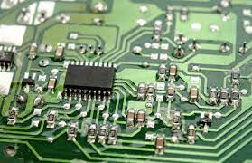
What is PCB substrate?
Every home is required to have a solid foundation. A substrate is also required for every printed circuit board. The actual substance that contains the traces and elements is known as the PCB Fabrication substrate. The first step in creating a high-quality PCB is selecting the correct substrate. Structure and shape are required for a PCB. It also requires a platform or canvas on which to place all of its other components. The PCB’s performance is influenced by the substrate’s properties. A stiff substrate, for example, can improve the PCB’s strength and endurance. More design options are available with a flexible substrate.
The usage of a variety of substrates, ranging from solid fiberglass to flexible polymers, is becoming more common as the PCB industry evolves. Fiberglass has traditionally been the most prevalent type of substrate. It’s a low-cost, high-reliability material that gives the PCB a nice, stable foundation.
Material of PCB substrate
It’s only reasonable that the materials you choose have an impact on your product’s performance. It’s the same with printed circuit boards, where selecting the correct PCB substrate materials can have a significant impact on the board’s performance, durability, and other characteristics.
Types of PCB substrate material
Following are the good material that we need for PCB substrate.
1. Copper foil:
PCB substrate materials are critical in defining the board’s endurance and quality. Manufacturers appear to be attempting to go towards fine lines and high density. You may be familiar with the term HDI PCB. This is the abbreviation of High-Density Interconnect Printed Circuit Board. To be classed in the HDI category ten years ago, a board had to have a line space (S) and line width (L) of less than 0.1mm. Today’s standards differ from one industry to the next. S and L on electronic devices are frequently set as low as 60m, and in advanced applications, they can even go as low as 40m. Once a thin copper foil substrate is applied, S and L can reach as low as 30m during circuit design development. The ideal thickness is between 9 and 12 meters.
The issue is that a thin copper-coated laminate can be costly and prone to flaws. It’s the most plausible explanation for why corporations use 18-meter-thick copper foil. However, if S and L are less than 20m, normal thickness copper foil may not be the best option.

2. Dielectric Insulating Coatings:
The ability to build up is a key feature of HDI printed circuit boards. There’s a good probability you’ll be able to construct an appropriate circuit if you utilize resin-coated copper (RCC) or combine copper foil lamination with epoxy glass prepreg cloth. MSPA and SAP techniques have also been implemented by the manufacturers. By using an insulating dielectric film lamination with chemical copper plating, the copper conducting plane was created. The fundamental reason we can make acceptable circuits is because of the thin copper plane.
3. High heat protection and dissolution are required:
Electronic devices tend to generate more heat as the trend toward downsizing and high function continues; hence thermal management of electronic devices is becoming increasingly important. Thermal-conducting PCB research and development is one of the solutions to this problem. The main criteria for a PC Board to operate well in terms of heat resistance and dissipation are the substrate’s heat resistance and dissipation capacity. Improvements in thermal-conducting capabilities of PCBs are now being made through epoxy and filler additions; however this only works in a limited category. The most common way is to use IMS or metal core PCBs as a heating component. This system has several advantages over the typical radiator and fan, including a smaller amount and lower cost.
How to Select Substrate Materials for PCBs
You can choose between three distinct types of PCBs:
• Rigid
• Flexible
• Flex-rigid
The most important goal is to select a board that is ideal for your product. Many people strive for compact size and shape while overlooking performance. Polyimide film is a good choice since it is adaptable and can be used in a variety of applications, including black, white, and transparent. It also ensures a low coefficient of thermal expansion while keeping acceptable heat resistance. The Mylar substrate, on the other hand, is extremely flexible and resistant to external conditions. Furthermore, it is reasonably priced, which is why many consumers consider it. Flexible PCBs must attempt to achieve the same degree of frequency and speed performance as regular PCBs. Flexible boards can be made with advanced polyimide substrates and polytetrafluoroethylene.
Flexible boards are used in a variety of industries, including medicine, smartphones, and gadgets. As a result, the market has been implementing innovations in flexible and ultra-thin multi-layer boards (0.2-0.4mm). You can expect flexible boards to achieve speeds of up to 5Gbps at this time, but you’ll need to choose a substrate material with a low Dk/Df. It’s also a good idea to utilize conductors with a thickness of above 100m, as this will aid with current and power handling.
Best PCB substrate type
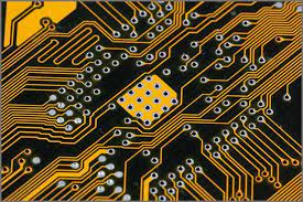
A substrate and printed wires are the two main components of a PCB (the copper traces). Substrates that divide the layers are required for multi-layer boards. The substrate works as physical support for the circuit components and printed wires, as well as providing electrical insulation between conductive portions. PCB Substrates are non-conducting materials. They act as a laminated electrical insulator between circuits for this purpose. An electrical insulator is a material that does not conduct electricity because its internal electric charge does not flow freely. As a result, plated through holes are used to connect traces on opposite layers on each layer of circuitry.
A substrate and laminate are commonly used as the foundation or base of a printed circuit board (PCB). The performance of the PCB is determined by the type of laminate and substrate used. As a result, choosing the proper types of PCB material for the job is crucial to getting the greatest results. Any PCB design guide should include such features:
Working
Durability
Cost-effectiveness
The material you choose for your PCB can have an impact on its short- and long-term functionality, along with your contractor’s capacity to build it. You can’t blame the contractor if you buy substandard materials and they fail when your contractor tries to make the board. When maximum performance isn’t a must-have feature for a PCB, lightweight polyester material is typically a fine option. As long as lightweight polyester is utilized in conjunction with printed electronics (PE) technology, there are at least two reasons to choose it in these circumstances. Printed electronics with lightweight polyester have these features:
Cost-effective Lightweight polyester produces less waste, necessitates fewer manufacturing steps, and eliminates the need for desalination and purification.
Adaptability Flexible printed circuits (FPCs) are available, but the level of “bendability” that makes them so appealing is costly to accomplish. PE with lightweight polyester maintains flexibility at a far cheaper cost.
Traditional PCBs, on the other hand, is still the top choice for high-performance applications, and the materials used in their construction should be determined by the type of board required. For example:
Manage frequencies ranging from 500MHz to 2GHz
Allow for high power and, as a result, high temperatures
Be “intense” and complicated
Manage microwave and above-microwave frequencies
The board’s application decides the substrates and laminates to utilize to a considerable extent. There are five types of substrates, each with its own set of features for specialized purposes.
1. FR-4
Fiberglass substrates are comprised of woven fiberglass that has been impregnated with only a flame-retardant substance. The material is rigid and can be drilled, cut, or machined, although tungsten carbide tools are required due to the abrasive nature of the fiberglass. An FR-4 substrate is more resistant to cracking or breaking than an FR-2 substrate and is typically seen in higher-end devices.
2. RF
Low dielectric polymers are employed in RF substrates, which are used in printed circuit boards for high-power radio frequency applications. Despite its low mechanical qualities, the substrate exhibits remarkable electrical performance.
3. FR-2
This extremely low substrate is comprised of impregnated paper, also known as Phenolic, and is simple to the machine over a fiberglass substrate. Flame Resistant is denoted by the letter “FR.” This substrate is commonly encountered in lower-cost consumer devices.
4. Flex
Flex circuits are those that are meant to be very flexible or slightly flexible. As substrates, thin, flexible polymers are used. Although the manufacturing process is more complicated than utilizing rigid substrates, it provides benefits that rigid substrates cannot, such as reducing space by bending the circuit board to fit a specific place or where repetitive action is essential. A low-thermal resistance substrate is required for power electronics. A ceramic core or metalcore substrate has the essential properties to accommodate larger copper tracks and the high electrical currents that these circuit boards require.
Final Thoughts
Every substrate has its uniqueness and you get to know almost every substrate detail in this write-up. Interested to know more about our facilities at PNC? Contact us at sales@pnconline.com


