Tag Archives: PCB Fabrication

3d-printed-pcb-prototype

Accelerate your New Product Development with rapid PCB assembly prototyping

The time from concept to prototype has accelerated remarkably in the past decade. 3D printed prototype components in a wide variety of materials are available in hours. Machined or sheet metal components are available from rapid prototype shops in only one or two days.

Prototype Printed Circuit Board Fabrication and assembly companies like PNC have followed this trend towards faster prototypes and can now provide complete assemblies in less time than ever before. PNC can fabricate and deliver a bare 10-12-layer PCB in just three days, and a simple double-sided board in just 24 hours.

However, even with the streamlining of PCB fabrication, the fully assembled PCBA is often the longest lead component in prototype designs primarily because of the sheer number and variety of passive and active components to be purchased and the demands of accurately placing and soldering those components. Sourcing the components on a typical PCBA BOM can take days in the best case and weeks in the worst case. Setting up and running the assembly job can add another few days, especially for double sided PCBs, and PCBs with a combination of surface mounted and through hole components.

Fortunately, there are some things that a product development team can do to reduce PCB assembly lead time.

First, do everything possible to reduce the impact of long component lead times. Plan to order the components as early as possible in the circuit design process. Deciding when to order components requires balancing the costs of scrapping some components as the design matures vs. the benefits of reducing the lead time for an assembled PCBA by days or weeks.

Second, reduce the time required to set up and build the prototypes by working with a full-service company like PNC. PNC has the capability to both fabricate the bare PCB and assemble the components. This means that the PCB fabrication team and assembly team can save time by working in parallel. While the PCBS are being fabricated, PNC’s engineers can create pick and place data, solder paste stencils and program the assembly equipment. When the PCBs are finished and the components arrive, everything is ready to begin assembly immediately.

The third way to save time with PCB prototypes is to minimize the number of PCB prototype iterations. Saving a full printed circuit board assembly prototype cycle is the most effective way to reduce the time from concept to mature design.

One way to reduce design iterations is by testing circuit designs as early in the design process as possible by building “Works Like” prototypes. “Works Like” prototypes are usually combinations of development kits, large one or two layer PCBs with larger SMT components that can be soldered by hand and various types of breadboards. In addition to testing the circuit, a “Works Like” prototype gives software developers an early platform to start developing code and debugging the circuit design. The result of testing early with rough prototypes is that you fix problems before you have invested the time in the full layout and prototyping process.

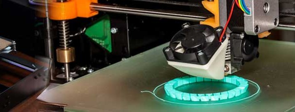
In parallel, the mechanical engineers can optimize cable routing and connector placement by printing 3D models of the PCBs, then epoxying actual connectors to the board model. This is an effective way to quickly try different options for cable routing using actual cables and connectors, since it is difficult to simulate the way actual cables behave with CAD software.

Experienced electrical engineers know that it is often poor connector access or cable interference that drive Printed Circuit Board layout redesigns as often as issues with actual circuit performance.

Once the circuit has been tested with the “Works-Like” prototype, and the board layout has been tested with 3D printed models, the last way to save time is to work closely with the PCB manufacturer to make sure that the PCB fabrication files are clean and complete, and that the BOM is accurate and matched with the circuit and layout to avoid placement mistakes.

This is another reason to select a full-service prototype pcb manufacturer like PNC. PNC can be a partner during the layout and design process, though fabrication and assembly ensuring the final design can be translated into a working prototype in the least possible time.


CONFORMAL-COATING

CONFORMAL COATING

What is Conformal Coating?

Conformal coating is protective chemical material coating applied after the final SMT PCB assembly or through-hole assembly process. Coatings are comprised of 5 different types, Acrylic, Epoxy, Urethane, Silicone and Parylene resins. Applying the coatings to a PCB board assembly can be done by hand spray, robotic spray, brush or dipping. The coating acts as an additional dielectric layer that provides protection due to environmental and mechanical stresses, such as thermal extremes, chemicals, dust, salt fog, abrasions, and moisture. In a PCB assembly that has close spacing of conductive pathways or close spacing of components the coating will help minimize dendrite growth over a period of time that causes shorting.

conformal_coating

Robotic Spray vs Traditional applications:

The method of application will depend on the customer requirements of the turnkey pcb assembly, but PNC prefers spray method for consistency in overall coating thickness. There are often select components on a pcb board assembly that will not be required to be coated. The traditional way is to block out or mask the selected components with tape. This is time consuming, costly and a possibility that the component can be damaged on the SMT assembly when removing. The robotic method can be programmed accurately to spray around the parts thus ensuring no component damage from masking and maintain a repeatable coating thickness.

When choosing a conformal coating for your turnkey pcb assembly, there are many manufacturers to choose from. The following are a few that we work with, Dymax, HumiSeal, Dow Corning, Hysol, Loctite, and Huntsman. Based on your application and environment of your PCB assembly, choose the Type of coating that fits the PCB board assembly, by visiting their web pages to find the strengths and weaknesses.

IPC J-STD-001D Conformal Coating thickness requirements

Type AR Acrylic Resin 0.03 – 0.13 mm (0.00118 – 0.00512 in)
Type ER Epoxy Resin 0.03 – 0.13 mm (0.00118 – 0.00512 in)
Type UR Urethane Resin 0.03 – 0.13 mm (0.00118 – 0.00512 in)
Type SR Silicone Resin 0.05 – 0.21 mm (0.00197 – 0.00827 in)
Type XY Parylene Resin 0.01 – 0.05 mm (0.000394 – 0.00197 in)

pcb manufactuter USA

Let PNC Simplify Your Printed Circuit Board Design With, CPLDs

New product designs continue to get more compact, while the performance and the number of features that customers expect continue to increase. To the engineer, this means higher PCB circuit densities and less room on the PCB for just-in-case design, such as unallocated I/O, or 0 ohm resistor networks to allow for reconfiguration of the PCBs at PCB assembly.

Meanwhile, new product prototype cycles are also getting faster. 3D printed mechanical parts are available within hours, putting pressure on electrical engineers to work faster and get their PCB designs right the first time. Even the fastest PCB fabrication, such as PNC’s 24-hour fabrication turn-time can’t help if the PCB has to be redesigned to fix errors.

The answer to both problems may be the CPLD. PNC’s CPLD programmers can help engineers reduce PCB size and allow on the fly circuit reconfiguration. Most people know that PNC specializes in fast PCB prototyping, but PNC is more than aPCB Manufacturer, PNC can speed prototyping by designing PCBs that replace inflexible circuit designs with PCBS that can be reconfigured to remap I/Os or change the order that circuit elements power up. A CPLD design developed by PNC can also allow the same PCB to be reconfigured to be used for the next generation product.

When it comes to programmable circuit elements, FPGA and microprocessors get all the good press. They are powerful, versatile, and generate more revenue for the manufacturers than workhorses such as CPLDS. Even though CPLD capability has improved dramatically over years, while both cost and power consumption have dropped, they are still often considered only for low level tasks such as “Glue Logic.” PNC designers can tell you that even a CPLD used for “low level” glue logic is appreciated when a late breaking design change means that two outputs now need to be two inputs, and one input needs to be inverted. All in a day’s work for PNC.

A PC Board Manufacturer, such as PNC can help you use these new, more capable CPLDs in places that can solve tough problems, replacing more expensive, complex and power-hungry solutions. Here are four examples.

I/O expansion

One of the most common CPLD applications is to expand the number of available microprocessor I/O ports. The CPLD I/O can either be multiplexed to the microprocessor or controlled via a serial interface. The advantage of a serial bus interface is that it allows you to locate this extra I/O anywhere, even on another Printed Circuit Board through a compact two or three pin connector.

The CPLD combinational logic architecture allows the creation of either a big fan-in or fan-out (over a hundred ports in some cases), and the outputs have enough current to drive small LEDS, a great way to create an array of circuit status LEDS.

When the CPLD output is used in conjunction with a CPLD’s internal clock the CPLD can also drive multiple PWM outputs allowing it to control things such as LED brightness, cooling fan speed, and simple sound producing devices.

The CPLD’s architecture gives it another useful capability for I/O expansion, the ability to accept inputs and drive outputs at different voltages. This multi voltage capability is often utilized for another common application; the communication bridge.

Bridges

CPLDs are often used as a bridge between one or more bus protocols, potentially at different voltages. They can support

  • serial to serial
  • serial to parallel,
  • parallel to parallel

They can even be used to drive an LCD. Because of their simple architecture, they have a low pin delay, making high speed synchronization possible.

Power Management

Another one of CPLD’s features is that they retain their programming and will boot within 500 µs. This means that the CPLD is the first programmable element to wake up on power up, so that it is awake and ready to manage the power up of power supplies and programmable devices ensuring they start in the right order.

Safety Systems

Because of the CPLDs simple architecture and 100% deterministic behavior CPLDs are often used in safety critical systems. One example application is to monitor interlocks, ensuring that the system is in a safe condition before the system can begin operation.

CPLDs pack a lot of capabilities into a compact package, they can reduce PCB complexity and allow reconfiguration on the fly. If you have never considered a CPLD in your design, the designers at PNC can help you with the CPLD circuit design, CPLD programming and Circuit board fabrication. Talk to PNC today.

Printed Circuit Board thickness considerations and requirements

How Do You Select a Printed Circuit Board Thickness?

Selecting the correct PC Board thickness for your product requires balancing of three often competing aspects of the design: manufacturability, electrical performance and mechanical constraints. Modern PCB fabrication techniques at PNC give the PCB designer great flexibility in specifying the PCB lamination stack-up and gives them the option to design a PCB in a thickness other than the typical choices of .031”, 062” or .093”.

Manufacturing considerations in selecting a PCB thickness

To understand how to specify PCB thickness, it is important to understand how PCBs are fabricated. Most multilayer PCBS from 2 layers to 40 layers are constructed of these three basic materials.

  • Core – a fully cured fiberglass panel usually with copper foil on both sides. It is essentially a two-sided Printed Circuit Board. PNC stocks cores in a variety of materials and thicknesses, down to 3 mils thick.
  • Prepregs – fiberglass sheets impregnated with uncured epoxy resin. This resin will cure and harden when subjected to heat and pressure during the lamination process. It is the functional equivalent of double-sided tape. PNC also stocks prepregs in a variety of materials and thicknesses.
  • Copper foil – used to create conductive layers. Copper foil thickness is chosen by the amount of current the traces in each layer of the board will need to carry.

Multilayer boards can be manufactured in a variety of thicknesses by mixing standard core thicknesses with standard prepreg thicknesses. The lower limit of PCB thickness is set by the number of layers and the minimum available core and prepreg thicknesses. Copper foil thickness also plays a small role in overall PC Board thickness.

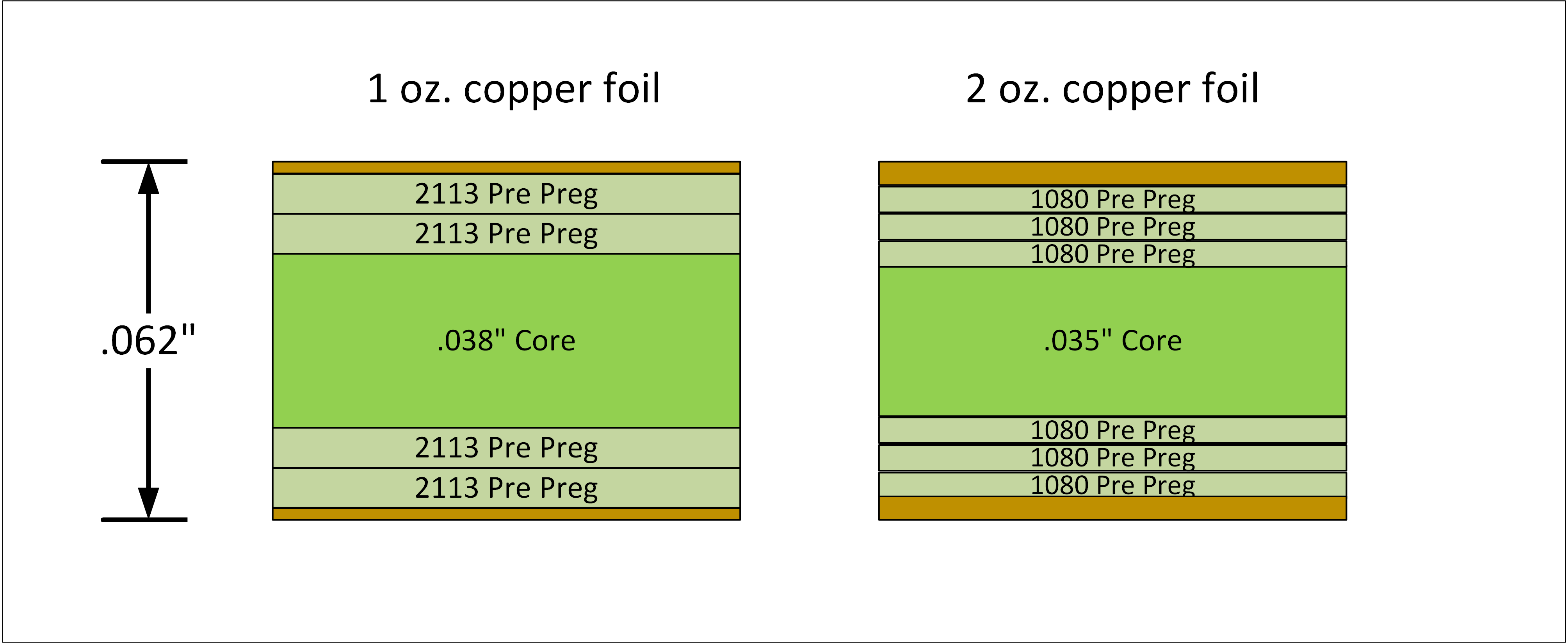
Providing you want to stay with the standard thicknesses, I’ll give you an example of PNC’s standard core thicknesses based off the core copper thickness. Let’s take an .062 and compare the stack-ups. See Figure  below:

Stack-up for an .062 multilayer:
062 thick PCB (002)


Notice to achieve the .062 overall thickness, the core thickness needs to be compensated based on the copper weight of the design. When using 1 oz copper we would use .038 core and .035 core for 2 oz. Also, the amount of pre preg would need to be adjusted as well to get to the thickness required. This is just one example when trying to determine overall thickness of your PCB.

The maximum PCB thickness is usually governed by something called the drill aspect ratio, which is the ratio of a drilled holes depth vs its diameter. When a hole is drilled, the deeper the holes becomes the harder it is to guide the drill accurately (because the drill deflects as it is pushed through the material) until you eventually reach a limit where you can no longer guarantee that the resulting drill hole will be centered in all the pads through the PCB. This is also referred to as drill wander in the PC Board fabrication world.

The aspect ratio for a through hole is the (board thickness) / (drill hole diameter).

Typically, the ratio is limited to approximately 10:1 This means that for a .062” thick board the smallest through-hole drill size is .006” which is the minimum drill size available at PNC. For a .093” thick PCB the smallest drill hole size will be .009” As board thickness increases, more complex via creation techniques such as laser drilled microvias are required to maintain the required pad density under components such as BGAs.

PCB thickness considerations for high speed circuits

One of the assumptions an electrical engineer makes when designing a circuit is that the PCB itself does not contribute any impedance to the circuit. However, in high-speed PCB design the integrity of the signals is definitely affected by the physical characteristics of the PCB.

Unfortunately for the designer the primary sources of parasitic capacitance and inductance of a PCB are affected by board thickness in conflicting ways, forcing the designer to carefully consider the trade-offs.

Vias

PCB vias can introduce both inductance and capacitance to the high-speed circuit. Parasitic inductance and capacitance of a via both increase proportional to board thickness.

Capacitance between layers
The capacitance between traces on different board layers or between traces and the ground plane are inversely proportional to the thickness of the dielectric between them. More space between layers will reduce parasitic capacitance and ensuring that all high-speed signal traces are the same distance from the ground plane will help impedance matching between them.

Crosstalk

Crosstalk between signal traces can be minimized by routing the PCB traces further apart and reducing the dielectric thickness between PCB trace and reference plane.

Mechanical Constraints

A PCB is ultimately a mechanical component of the product and is therefore subject to a variety of mechanical constraints. The PCB or PCBs must fit within the product envelope. This often requires that a PCB be as thin as possible. On the other hand, PCBs are subject to the torqueing forces from cables connected to the board edge and external connections. Preventing board failure during assembly or in use requires a circuit board fabrication thick enough to withstand these forces.

Finally, PCBs in the field are subjected to both vibration and shock. For example, large PCB panels can vibrate in several different modes when subjected to vehicle vibration, causing fatigue and eventual failure of solder joints. The rule of thumb is to get the resonance modes of a PCB to be 10X the input vibration. This requires designing thicker, stiffer PCBS and by careful placement and design of the PCB mounts.

These are the three most important considerations in selecting a PCB thickness. To optimize a PCB design, the PCB designer needs to understand all of these requirements and constrains on the PCB lamination stack-up, and have the flexibility to choose a PCB thickness that balances these often conflicting constraints. The team at PNC can help you design a PCB that meets your needs at a competitive cost and lead time.