Tag Archives: pcb assembly manufacturer

pcb manufactuter USA

Let PNC Simplify Your Printed Circuit Board Design With, CPLDs

New product designs continue to get more compact, while the performance and the number of features that customers expect continue to increase. To the engineer, this means higher PCB circuit densities and less room on the PCB for just-in-case design, such as unallocated I/O, or 0 ohm resistor networks to allow for reconfiguration of the PCBs at PCB assembly.

Meanwhile, new product prototype cycles are also getting faster. 3D printed mechanical parts are available within hours, putting pressure on electrical engineers to work faster and get their PCB designs right the first time. Even the fastest PCB fabrication, such as PNC’s 24-hour fabrication turn-time can’t help if the PCB has to be redesigned to fix errors.

The answer to both problems may be the CPLD. PNC’s CPLD programmers can help engineers reduce PCB size and allow on the fly circuit reconfiguration. Most people know that PNC specializes in fast PCB prototyping, but PNC is more than aPCB Manufacturer, PNC can speed prototyping by designing PCBs that replace inflexible circuit designs with PCBS that can be reconfigured to remap I/Os or change the order that circuit elements power up. A CPLD design developed by PNC can also allow the same PCB to be reconfigured to be used for the next generation product.

When it comes to programmable circuit elements, FPGA and microprocessors get all the good press. They are powerful, versatile, and generate more revenue for the manufacturers than workhorses such as CPLDS. Even though CPLD capability has improved dramatically over years, while both cost and power consumption have dropped, they are still often considered only for low level tasks such as “Glue Logic.” PNC designers can tell you that even a CPLD used for “low level” glue logic is appreciated when a late breaking design change means that two outputs now need to be two inputs, and one input needs to be inverted. All in a day’s work for PNC.

A PC Board Manufacturer, such as PNC can help you use these new, more capable CPLDs in places that can solve tough problems, replacing more expensive, complex and power-hungry solutions. Here are four examples.

I/O expansion

One of the most common CPLD applications is to expand the number of available microprocessor I/O ports. The CPLD I/O can either be multiplexed to the microprocessor or controlled via a serial interface. The advantage of a serial bus interface is that it allows you to locate this extra I/O anywhere, even on another Printed Circuit Board through a compact two or three pin connector.

The CPLD combinational logic architecture allows the creation of either a big fan-in or fan-out (over a hundred ports in some cases), and the outputs have enough current to drive small LEDS, a great way to create an array of circuit status LEDS.

When the CPLD output is used in conjunction with a CPLD’s internal clock the CPLD can also drive multiple PWM outputs allowing it to control things such as LED brightness, cooling fan speed, and simple sound producing devices.

The CPLD’s architecture gives it another useful capability for I/O expansion, the ability to accept inputs and drive outputs at different voltages. This multi voltage capability is often utilized for another common application; the communication bridge.

Bridges

CPLDs are often used as a bridge between one or more bus protocols, potentially at different voltages. They can support

  • serial to serial
  • serial to parallel,
  • parallel to parallel

They can even be used to drive an LCD. Because of their simple architecture, they have a low pin delay, making high speed synchronization possible.

Power Management

Another one of CPLD’s features is that they retain their programming and will boot within 500 µs. This means that the CPLD is the first programmable element to wake up on power up, so that it is awake and ready to manage the power up of power supplies and programmable devices ensuring they start in the right order.

Safety Systems

Because of the CPLDs simple architecture and 100% deterministic behavior CPLDs are often used in safety critical systems. One example application is to monitor interlocks, ensuring that the system is in a safe condition before the system can begin operation.

CPLDs pack a lot of capabilities into a compact package, they can reduce PCB complexity and allow reconfiguration on the fly. If you have never considered a CPLD in your design, the designers at PNC can help you with the CPLD circuit design, CPLD programming and Circuit board fabrication. Talk to PNC today.


Telescope

Ensuring a successful Turnkey PCB Assembly project

There are many detailed factors involved when pursuing the right company for your electronic or PCB assembly needs. These factors can be broken down into two distinct areas, customer communication and supplier contract review. Either the customer or the supplier cannot afford time lost if there is a misunderstanding or lack of data to efficiently and effectively produce a quality product on time. Time spent up front makes for a smooth and efficient transition through the quoting and manufacturing process.

Customer communication

A majority of communications for a request for quote, RFQ’s, in today’s industry are via email. The email needs to contain the required data files and be clear and concise in regard to quantities and delivery dates, along with any details that are not stated on the fabrication/assembly drawings. Since we are talking about Printed Circuit Board Assembly Turnkey projects, let’s break this down further with the required data files for PCB and PCBA.

PCB data files:

1- Fab drawing with build details such as material type, thickness, Copper weight, Tg rating, IPC-A-600 Class, Stack-up, Drill Chart, LPI & silk screen color, Serialization, Panelization array, MIL Spec, final finish and type(RoHs/Non RoHs) etc.
2- Complete set of gerber files.
3- Drill files.
4- IPC-356 Netlist for electrical testing.
5- Read me file for additional information not stated in fabrication drawing or email.

PCB Assembly data files:

1- BOM with manufacturers part number/description and alternates if applicable or DNP’s.
2- Assembly drawing with build details, Solder paste requirements, torque specs, IPC-A-610 Class, DNP’s, serialization, etc.
3- Pick & Place file.
4- ICT or Probe testing if applicable.
5- Functional test procedure if applicable.
6- Read me file additional information not stated in fabrication drawing or email.
If all the required information and data files are complete, we have successfully met the first half of the RFQ process. With this in mind, it’s up to us to compile this information in our contract review process. Let’s take a look at what is processed on our end to complete the RFQ cycle.

Supplier Contract review

All incoming turnkey projects are given an internal number for uniqueness especially for part numbers that has been revised. They are stored in a secure file folder based on two groups of data. ITAR data is stored separately than non-ITAR data. Once the customers data is stored and secure, engineering is notified to start to contract review process for the PCB and PCBA data sets.

Contract review for PCB:

1- Gerber files are imported and overlaid into correct layer structure.
2- Drill files are imported and overlaid against the gerbers.
3- If there is no IPC-356 Net list file, we extract the net from the gerber.
4- The gerbers are ran through a design rule check for manufacturability.
5- Fab drawing is reviewed by engineering for manufacturing capability.
6- If any discrepancies are determined, customer is notified immediately, If no discrepancies, engineering hands off the internal contract review check sheet to customer service.

Contract review for PCB Assembly:

1- BOM is scrubbed to ensure all parts are identified by manufacturer and P/N.
2- BOM parts stock research from approved vendor list.
3- Assembly drawing reviewed by engineering for assembly capability.
4- Pick & Place file review.
5- Review for testing if applicable.
6- If any discrepancies are determined, customer is notified immediately, If no discrepancies, engineering notifies customer service.
7- Quoting team is notified to officially create the quote and send to customer.
Customer communication and supplier contract review is a relatively simple step in order to achieve and ensure a successful assembly turnkey project. Adhering to the steps above can make for a great partnership.

Grounding in Printed Circuit Board Design

PNC-main-mid2

As we advance into the future, we want everything to be faster, cheaper, compact and durable. Everything around us is electrical. Moore’s law predicted that numbers of transistors per square inch of Printed Circuit Board will double every 2 years and it’s been true too date. Well theoretically it sounds good. But implementing new products with the above requirement comes with a cost. In order to reduce the unit cost of the design, due to noise. Various techniques have been developed in the past few decades to reduce noise in the circuits as the number of components increases and the available size decreases. Design techniques include proper grounding, decoupling, routing and signal multiplexing.

Grounding at PCB level can be in implemented as single point ground. As the name suggests a single point ground is where the complete circuit residing on the PCB has a single ground. This technique is developed by using a ground plane. Ground plane is defined as a highly conductive electrical surface which will be used as a system ground. In printed circuit boards, it is referred to as a large conducting surface of copper foil on either side of the PCB. It is connected to the power supply ground terminal and thus it serves as a return path for current from different components on the board .The fact that a large surface area of highly conductive metal, like copper, has a very low impedance which forms the basis of this method.

Ground plane is laid on the PCB, such that it covers the maximum area which is not occupied by circuitry itself. In multilayer PCB’s, it is often a separate layer covering the entire board. This makes the circuit design easy to implement, thus further allowing the designer to ground any component or subpart of a circuit without adding additional traces. The large area of copper which provides a very low impedance path conducts the large currents originating from other components/subparts without significant voltage drops. This ensures that the ground connection of all the components is at the same reference potential.

request-for-more-info-button1

Benefits of grounding in PCB are:

  • Reducing electrical noise
  • Reduce interference being coupled from one part of the circuit to another.
  • Reducing crosstalk between adjacent circuit traces.

1) Noise reduction:

When circuits switch states, large current flows from the active devices through the ground. If the power supply and ground traces have noticeable impedance, then the voltage drop across them may create noise voltage that would disturb other parts of the circuit. The large conducting area of the ground plane has much lower impedance than a circuit trace, so the current causes less disturbance.

2) Interference & Crosstalk reduction:

When two traces are placed too close to each other, an electrical signal in one can be coupled into the other. This is due to electromagnetic induction caused by the linking of magnetic field lines from one trace to other. This phenomenon is known as crosstalk. When a ground plane layer is present underneath the circuit in the PCB, it acts as a transmission line for the trace. Thus the direction of current flowing through the ground plane is opposite to the direction of current flowing through the circuit trace. This cancels most of the electromagnetic fields and consequently reduces crosstalk.

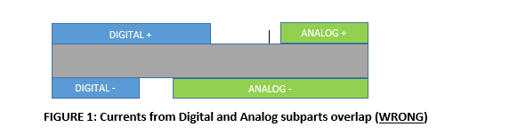
Many of the present day circuits consist of both Analog and Digital subparts. To avoid current from one subpart to affect the other subpart, ground planes are split and then connected by a thin trace. The thin trace has low enough impedance to keep the two sides very close to the same potential while keeping the ground currents of one side from coupling into the other side, completing a ground loop.

11

21

Thus grounding in PCB can significantly improve the circuit/chip performance. No extra area is added to the chip as leftover areas are used. This method doesn’t add too much of cost to the initial design which makes it readily acceptable at industry level.

Types of single ground connection:

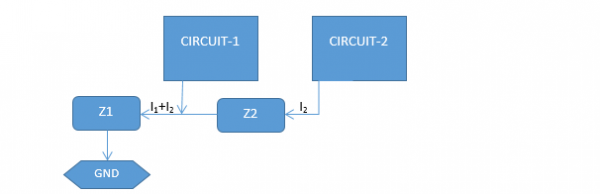
    • Series Ground Connection:

31

    • Parallel Ground Connection

41

Terry