Tag Archives: pcb board assembly

PC Board Fabrication for High-Speed Circuits

PC Board Fabrication for High-Speed Circuits in Pcb Assembly

PC Board Fabrication for High-Speed Circuits?
PC Board Fabrication

If you have seen printed circuit boards (well, I am sure you have seen one) then you must wonder how they are made and how they are managing your electrical devices. Nowadays, a multiple-layer printed circuit board is managing the most critical electronic devices. From your laptop to your phone and other devices are relying completely on printed circuit boards. Printed circuit boards may seem uninteresting to you but once you get deep into it, it’s an interesting and worth knowing subject. Let’s imagine, how a printed circuit board is working in the device you are using right now, and it will boost your interest. Now the question may arise about the manufacturing of the circuit board. How is a printed circuit board manufactured and prepared?

There are few rules in the designing and manufacturing of printed circuit boards that need to be followed. The material being used in the circuit board matters a lot. The main purpose of the material is to provide insulation between the conducting layers of the copper foil and pass electricity. Essentially four basic layers need to be followed in manufacturing a printed circuit board. The format of these layers is:
• Silkscreen
• Solder mask
• Copper
• Substrate

Initially, there were only two choices available for the PCB’s. One is a rigid circuit and the oter is a flexible circuit. Now as the electronics industry has been developed the boom in printed circuit boards can also be seen easily. Now we have a choice of different printed circuit boards for different devices. For example, various frequency ranges and antennas.

But the thing that needs attention is that the base material used in the manufacturing process of printed circuit boards is still the same. And the material used as a base for the printed circuit board still falls into the rigid category of the printed circuit boards. Now let’s understand what a substrate is.

What is the substrate?

Let’s imagine a building. What is the base of the building on which it is relying entirely? The ground, right? Similarly for the manufacturing of printed circuit boards, we need to build a base first. And the same as the building should have a reliable and strong ground, the printed circuit board also requires a good and efficient material with a number of characteristics in order to stand out in the world of electronics.

The substrate is the first physical layer of the circuit board on which the traces and components are relying. If you want to manufacture a reliable and high-quality printed circuit board, choosing the right and recommended material for the substrate layer is the first step you should go for. There are a variety of choices available when you get to choose the material of the substrate. But first, let’s understand why it is important to give this much attention to substrates.

Importance of substrate

There should be a solid shape and structure for the PC Board so that the other layers, traces, and components can easily rely on it. A strong canvas and platform are required to better hold all the components. The overall performance of the printed circuit board would be affected by the quality of the substrate. A soft substrate offers more space for designing options. On the other hand, hard and rigid substrates increase the durability of the circuit board. Similarly, if we need multiple designs on the printed circuit board then we may use multiple substrates for each layer. As we need to be concerned about the non-conductive material so the substrate decided should be able to withstand heat and dielectric constant also.

Now let’s have a look at different types of substrate with an explanation so you can understand how substrates are suitable in particular circuit boards. Moreover, the substrate is the reason for the stability of the printed circuit boards. It protects the board from bending by providing it with a hard or flexible surface. For example, the computer motherboard is probably the most common substrate you can see now. The motherboard is a multiple-layer printed circuit board. You can see that other components and traces are connected to the surface in such an efficient and best way.

Rigid Substrate:

As we have discussed before, the rigid substrate is always a good choice when we want a strong and dielectric circuit. Also, the rigid substrate can cross up to 350 degrees, so it is a noteworthy operating temperature. Rigid substrates are preferred when you want a PCB in a way that it can be repaired and maintained easily. It is easy to mark the affected area because of the clear view of the board. Rigid substrates are the best choice for critical situation usage devices for example LEDs used in medical surgeries. Ceramic-based substrates are the most common these days. Common examples are aluminum nitrate and aluminum. Rigid substrates offer high thermal stability and low expansion and are easier for the pcb assembly process.

Soft Substrate:

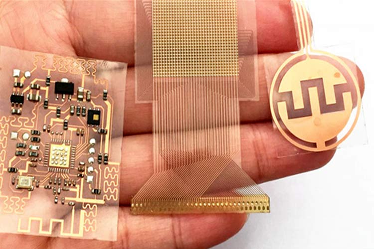
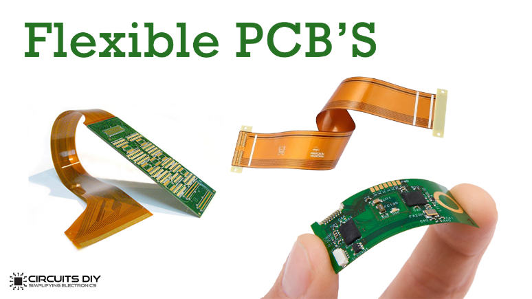
There are renowned benefits of using soft substrate in a printed circuit board. Soft substrate act as a shield in a hazardous environment. You can make a corrosion-proof, waterproof, and shockproof printed circuit board by using the soft substrate. This advantage is not provided by most rigid substrates. The dielectric material or glass material can be protected by epoxy coating around the filler. The soft substrate also provides resistance against chemicals and radiations. The melting point is high in them. Soft substrates have made the wearable concept possible. It is now possible to enable printed circuitry in tight areas just because of the soft substrate used in it. Although flexible material used in circuit boards is expensive, it provides better functionality by reducing the weight of the overall circuit.

Flex-Rigid substrate:

Sometimes a PCB requires easy fixation. Lightweight can also be a condition to follow. In this case, flex-rigid can accommodate the requirement perfectly. Specific flexible substrates such as R0400 are used in circuit board manufacturing; they are simple to machine and precision built. They are the most lightweight substrate, so it is possible to reduce weight and space up to 50 percent. Because of these features, flexible substrates are the best available choice for most printed circuit boards.

FR-4:

If you want to build a complex and multilayer printed circuit board then FR-4 is the way to go. They are also known as fire retardants, and they offer high resistance against flames because of the bromide present in them. There are several subcategories of FR-4 such as TG and FR-4 Roger. The other advantage of this substrate is that it is cost-friendly. Highly optimal performance of microwave frequency in the printed circuit board can be achieved by using RF-4 because of their strength to weight ratio. This is also a reason for their affordable design.

Now we have analyzed the reasons why we should go for good substrates. Let’s also understand the materials of the substrate. Because the quality of the substrate plays an important role in deciding the efficiency and reliability of the PCB as well as the end product.
Ceramic substrates are usually preferred because of the high magnitude of the thermal conductivity as compared to conventional printed circuit board material.

Commonly used substrate materials are Al2O3, AIN and FRx. alumina is preferred because it offers high resistivity, the best dielectric strength, good thermal and corrosion stability, and the best mechanical power. Its major disadvantage is a delay in propagation signal because of the relatively high rate of dielectric constant. It is also difficult to draw away heat and the reason is low thermal conductivity.

That’s why ceramic materials are under development. The main purpose of these developments is to improve the existing material. Integrated circuits are one of the best examples. As they perform complex functionality, it is important to build a printed circuit board with multiple layers. The low dielectric material is used in these circuits.

Similar polyimide is also used as a substrate in printed circuit boards. It offers wide temperature ranges and better chemical resistance. Its electrical properties are also good. Typically, these PCBs are used in cameras, antennas, entertainment devices, calculators, and instrumental panels. The other material that is recommended in the substrate is PTFE, this offers low dissipation and maximum temperature stability and would require a fixture for the printed circuit board assembly process. These are used in antennas, the aerospace industry, and power amplifiers.

There are many other examples of the best substrate materials that many industries are using for manufacturing better-printed circuit boards. The end goal is to provide stability and reliability under severe conditions. Also, it is preferred to use substrate material that is beneficial for critical industries and helpful in industries such as medical and aerospace.

The entire printed circuit board is relying on the substrate as it provides the basic foundation. The other components such as silkscreen, copper foils, and traces can do good if the basic physical layer is good. That’s the reason you should take some more time in deciding your substrate material and type. This will be a key to your PCB’s better performance.

Are you looking for the best substrate material for your PCB manufacturing and smt assembly? PNCONLINE is your ultimate solution. Just write us at sales@pnconline.com to get customized rates for your PCB manufacturing solutions.

Flexible Printed Circuit Board Overview

Introduction

On a slightly less romantic level, it would not be feasible to have such a standard laptop or mobile phone without flexible print circuit technology, which enables components to be linked electrically, in a dynamic, three-dimensional fashion. Flexible circuit technology has a long history that dates back over 100 years. The early patent activity emphasizes the fact that inventions such as Thomas Edison, Frank Sprague, and others in the early twentieth century experimented on ideas for flexible circuit materials and designs that were only used on a commercial basis in recent decades.

Background

Flexible printed circuits (FPCs) are the heart and soul of flexible films and thin layers of conducting traces. These typically represent the flexible circuit laminate base that can be used to connect electronic equipment – such as the LCD screen or a laptop’s keyboard – as a reliable cable replacement, or electronic components can be directly fitted to it through solder or conductive adhesive to form a completed, flexible printed circuit board.

Flexible printed circuits

Flexible PCB advantages

Flexible, FPCs may be bent and curved to provide more flexibility of application design and operation. Flexible circuits may also be adapted to tiny or inappropriately shaped areas, which cannot be supported by conventional rigid circuits. There is another benefit of flexible PC Board is that to reduce the weight of the motherboard of the application, they need less space. The effective utilization of existing areas also helps to improve thermal management and reduce the dissipation of heat.

Flexible PCBs may also be more dependable and longer-lasting compared to stiff PCBs, particularly in situations where constant vibration and mechanical stress are experienced. Based on soldered wires and hand-connected connector models, standard connecting methods are replaced by flexible printed circuits, with exceptional weight and thickness, and with strong mechanical resistance.

Think for example of connecting numerous electronic equipment, such as dashboards, display, and man-machine interfaces, in the automobile industry (rotary controls, buttons, etc.). All these gadgets are exposed to constant mechanical strains and vibrations and need a stable connection in all vehicle operating circumstances. Flexible printed circuits ensure zero reliability, durability, and maintenance in the automobile industry.

Flexible PCBs
Flexible PCBs

Flexible printed circuit boards provide a variety of possible advantages including:

  • Flexible PCBs provide cost-effective benefits that include decreased requirements for materials and packaging, reduced component replacement costs, and assembly mistakes that may lead to repair requirements.
  • These advantages make flex PCBs suitable for a broad variety of sectors, including consumer electronics, transport, medical, communications, military, automotive, industrial applications, and aerospace.

Missing Dielectric Material Callouts

Flexible and stiff flexible circuits are made utilizing a variety of material types to satisfy a broad range of physical and electrical costs and performance criteria. Because of this variation, the designer must give comprehensive information on the dielectric materials to be utilized about the potential problems associated with each choice. It is suggested that designers learn about the cost and performance options available. The Internet is filled with information about flexible circuit materials and how they may be utilized. This issue may also be helped by the PCB manufacturer. The fundamental kinds of flex materials are:

  • Adhesive materials without acrylic binding the copper to dielectric polyimide
  • Adhesive materials with acrylic copper bonding with dielectric polyimide
  • Flammable and non-flammable laminates, covers, and bonding flakes.

Incomplete or Insufficient Rigid-Flex Base Material Type Definition

The selected base material determines the rigid-flex circuit’s performance limitations in-process and field operation in many applications. For most solders devoid of plumage, the highest temperature requirements for soldering may be as high as 260°C, which usually requires the use of polyimide laminates. The choice of material and its electrical characteristics may, however, influence other performance problems.

One important issue is to control the characteristic impedance of the system and guarantee signal integrity with increasingly prevalent designs of higher-frequency circuits (these latter subjects will be given more attention later). The requirements for the temperature range of the stiff laminates used in rigid-flex structures must also be taken into account and handled. The stiff material should be capable of high temperatures. Polyimide laminate is a frequent callout, although epoxy resins are often appropriate for better applications.

Copper Type and Thickness Callout

Whilst many metal foils are available for flexible circuits, copper is the most frequently utilized metal for electronic interconnections. It is extremely conductive, mixable (making it flexible and foldable), reasonably easy to manufacture via graving and placing, and relatively cheap. The copper type most often used for flexible circuits is roll and copper (RA copper) with the greatest characteristics for dynamic flex applications.

The choice of type and thickness for the copper design should correspond to the electrical and mechanical requirements for use. Thicker copper is usually utilized for greater energy and thinner copper for circuits requiring repetitive bending (dynamic flexing). The options of thickness are many, but at present, one ounce (17μm or 0.7mils) and one ounce (35μm or 1 mil) are the most utilized for creating flexible circuit laminates. Additional copper may often be placed on the circuit, and this should also be taken into account in the specification. If the designer is unsure, he should seek the assistance of engineers for advice.

Flex Circuits
Flex Circuits

Cover layer or Solder Mask Over Flex Circuits

Covers are polymer materials used for the covering and protection of the copper traces of the flex circuit product. As is indicated, many solutions for the protection of the circuits are accessible and they meet various design criteria in terms of cost, performance, and flexural durability optimization. It is essential to describe the choice not only of the kind of cover material but also of the thickness required. This may be extremely significant for certain building types, especially when a flex circuit experiences dynamic flexing during usage.

As far as costs are concerned, a flexible solder mask is usually the cheapest. Someone or two-layer flexible circuits, which are not subjected to repeated flex cycles or severe radius curves, may be covered with a solder mask epoxy-based to flex without breaking. However, this is not advised if the design needs severe or dynamic flexing.

The second choice is the laminated cover. These materials are usually identical to the flexible core materials and are best suited for flexible dynamic circuit applications. The cover is a polyimide sheet with one side acrylic adhesive. It is usually pre-machined to open the sheet where the final finish is needed.

The cover sheets are typically coated with specific pads in a laminating machine to ensure that the copper characteristics of the flex layer are conformed. For rigid-flex circuits, the overlayer is usually reduced to not exceed 50 miles in the rigid part. The aim is to ensure that all the plated holes in the stiff-flex are empty of any acrylic adhesive, since they may influence the integrity of the hole wall plating.

Flexible Printed Circuit Board disadvantages

Although there are many significant benefits, the FPC technology also has several inconveniences or downsides. First and foremost, FPCs have significant one-time startup costs compared to conventional rigid PCBs. The initial expenses associated with the circuit and prototype design are greater than for rigid PCBs because flexible systems are developed for highly particular purposes. If the cost is a deciding factor in the choice of the kind of PCB, the use of FPC technology is preferable only for not too low manufacturing quantities.

The difficulty of fixing or changing the PCB when it is rebuilt is another drawback. In this situation, in reality, the protection film that covers the circuit must first be removed, the procedure carried out and protection restored. In order to provide their clients with this kind of product, flexible PCBs are quite a new technology and not all manufacturers are prepared. Moreover, considerable care must be exercised during the assembling stage, because the circuit may be easily destroyed by improper handling or by unauthorized people.

Structure

The historical electric connection methods have been revolutionized, typically for connecting various portions of the same circuit or different electronic devices by introducing flexible PCBs. The flexible PCB-based solution enables significant space, weight, and costs to be reduced compared to an equivalent solution using rigid PCBs due to its flexibility and compactness as well as the high density of electrical connections available. Many kinds of cable systems, frequently manual in multiple applications, have been replaced with flexible printed circuits which reduce overall electrical cable costs by up to 70%.

Interested in getting your Flexible PCB design ready at economical rates in USA? Get it done at PCNONLINE.

Final Thoughts

In the last few years, the FPC business has expanded significantly led by the development of wearable and electromedical devices that are increasingly tiny and light. Flexible PCBs may remove connector and cable requirements in many applications, enhance connection reliability and reduce assembly time, assembly cost, and total device sizes. We can state that flexible PCBs have enabled new in conclusion, fascinating applications to be implemented that are not possible with conventional rigid PCBs.

Flexible printed circuits, from cars, VCRs, camcorders, cell phones, and SLR cameras up to the complex military and aviation systems, are present in all areas. There are numerous high-profile uses of flexible circuits. One example is the employment of flexible-circuit technology in the Sojourner, a robot that explored the Mars surface and collected data in the summer of 1997, in the stiff flexible wire harnesses employed.

Do you have any further questions? Feel free to write us at sales@pnconline.com

Smt Assembly Conformal Coating

SMT Assembly Conformal Coating

Definition

Conformal coating is a thin layer of protected polymeric coating applied to printed circuit boards (PCBs) and electronic components. Its goal is to provide environmental and mechanical protection for the components and circuits, allowing them to last longer and be more reliable. It maintains long-term surface insulation resistance values by being electrically insulating, ensuring the assembly’s operational integrity. It also prevents corrosion by acting as a barrier to airborne pollutants from the operational environment, like salt spray.

Conformal coatings are often applied in the 25-250 micron range. Parylene films, on the other hand, are applied significantly thinner and can be fractions of a micron thick. Conformal coatings are a flexible covering that will secure the printed circuit board assembly from the environment it is in by filtering out air pollutants and ensuring long-term interface resistance value while also allowing any moisture trapped in the circuit board to dissipate.

The notion of conformal electronics coating was first conceived and refined through research decades ago to suit the rigorous requirements of the military. HumiSeal was a pioneer and leader in that early research and the company has remained a pioneer and leader for over 60 years as the technology has spread to a variety of industries, including:

  • Industrial Controls
  • Automobiles like Hybrid and Electric Vehicles
  • Aerospace
  • Telecoms
  • Traditional and renewable energy
  • White thing

 Conformal coating types

While there are many other types of coatings, including a few specialist forms, five primary categories are depending on the chemical makeup of the substances.

  1. Urethane Resin (UR):

Single-part or two-part urethane resins are available. It is chemically resistant as well as humidity resistance. On the other side, it is simple to remove and rework with a soldering iron.

  1. Acrylic Resin (AR):

Preformed acrylic polymers that have been dissolved in a solvent are known as acrylic. Typically, they are one-part compounds. It is inexpensive and simple to apply and remove. During the curing method, there is no distortion.

  1. Epoxy Resin (ER):

Epoxy coatings are typically two-part compounds, but a one-part option is also available. It has moistures. It performs admirably in adverse conditions.

  1. Silicone Resin (SR):

Silicone resin coatings are one-component materials that are frequently used on devices that will be exposed to severe temperatures. Even at high temperatures, it performs excellently. It can stick to almost any PCB material.

  1. Parylene (XY)

Chemical vapor deposition is the method used to apply parylene coatings. When heated, parylene turns into a gas. It is then placed in a vacuum chamber to polymerize and form a film after cooling. After that, the film is applied over the circuitry. It is translucent and colorless. It is the ideal solvent for coating and can be done at room temperature.

Uses of conformal coating

When today’s dynamic electronics are faced with significant environments, additional protection is required to ensure proper operation. Moisture, salt sprays, strong chemicals and solvents, vapors, dust, abrasion, and even organic assault have all been proved to be resistant to conformal coatings. Furthermore, it has been demonstrated that the impact of mechanical stress and disturbances on the circuit and its functionality in severe temperature ranges can be reduced by using the right material. Conformal coatings protect the product while also improving its reliability. As a result, the negative impacts of early field failures are reduced, as is the potential cost. We use conformal coating for:

  • It works as a moisture and humidity-resistant barrier, resulting in lower leakage currents, converse, and electrical and chemical transfer throughout the board.
  • The coating has the potential to improve the strength of dielectric conductors.
  • The coating provides a high level of insulation safety, allowing conductor space to be reduced.
  • It prevents the board from chemical and corrosive attacks that can cause corrosion. It also protects against damage caused by hard handling, as well as thermal and mechanical load.
  • The coating prevents particle pollutants from reaching the board’s surface.

 Method of conformal coating

The following are types of common Printed Circuit Board conformal coatings:

  1. Brushing

Brushing a conformal coating is a popular method of application. Although this is a simple procedure, it needs the use of a trained operator to ensure the coating’s quality and finish. A brush, a container for storing the coating, and a specified area for application are all required. The coating material is dipped in the brush and applied to the board.

The type of brush, operator competence, coating viscosity, the environment, and the coating material all affect the brushing method’s quality. It has many benefits, including ease of use, simplicity, and reduced process control needs. This method is ideal for rework and low-volume production. In this process, we use hands and are thicker and less pleasing artistically. This is the ideal option for individuals who don’t have the tools to use other options or who are working on a few boards at once.

  1. Spraying:

This procedure produces a better surface polish and is more cost-effective, but it does not penetrate the board deeply. Spraying, which is also preferable for low-volume production, is time-consuming because all parts that do not require coating must be masked. Spraying with aerosols, batch spraying, and selective spraying are all part of this approach.

A spray gun is included with an aerosol. It’s a coating with a solvent basis. Aerosol spraying in a spray booth is a low-cost option. This procedure is superior to brushing because of the inexpensive setup costs, high process speed, simplicity, and final quality.

Batch spraying utilizes a compressed air spray cannon to provide a high-quality coating finish. For the setup, you’ll need a spray gun, a spray booth, and an air compressor. In this operation, it’s crucial to get the spray gun set up with the right atomization pressure and material supply. It’s also crucial to get the coating’s viscosity just correct. It has features such as inexpensive setup costs and flexibility.

Spraying selectively only coatings selected areas. The coating isn’t applied to regions that need to be masked, like connectors and other components. The coating is done with the use of a customized robot system that uses various spray patterns. Valve selection, board material, and board arrangement are all important considerations. The correct spray valve and coating viscosity must be selected.

All sorts of conformal coatings are supported by the spray approach, and designing for this procedure necessitates a high level of technical knowledge. As a result, spray application requires significant capital expenditure. In addition, the material’s performance over time and changes in the control environment must be monitored.

  1. Dipping:

Dipping is the process of immersing a board in a coating solution and then removing it. This process is ideal for high-volume assembly since it is quick, precise, and penetrates the board, coating the entire assembly. However, to eliminate leakage, masking must be flawless, rendering many boards unsuitable owing to design. This approach can only be used on boards that take coating on both sides.

This is a conventional procedure that involves dipping the pcb assembly into a tank of coating chemicals. The speed of immersion, coating dwell time, and board withdrawal speed are the variables that determine the process. Acrylics and urethanes, which are solvent-based conformal coatings, are recommended for dipping. It’s a high-speed process that can be used in batch or in-line processes.

The conformal coating manufacturing process

In the conformal coating production process, there are eight main steps:

Cleaning:

The cleaning eliminates a variety of residues that result from operator handling, soldering, machine use, and pollution from the environment.

Priming:

Priming is the process of applying a preliminary coating to a board before applying the conformal coating. It improves adherence and produces a binding layer to keep the coating in place. The amount of priming required varies depending on the type of resin.

Masking:

The function of masking is to prevent the conformal coating from being placed on the parts and selected board sections. Because of the insulating nature of the coating, certain regions of the circuit board must remain uncoated. Many materials are used in masking.

Cure and dry:

There is a difference between Cure and dry. That is:

Cure:

This means that the coating achieves the desired qualities (electrical and mechanical) and that the board is protected while in use.

Dry:

This assures that the PCB is laminated and suitable for the users to operate. It could take anywhere from a few minutes to several days.

Checking:

In the procedure, it is the most crucial stage. Manual inspection, UV lamp visibility, and automated optical inspection are all included.

Benefits of conformal coating

When it comes to choosing parylene coating that meets standards, there are several clear advantages and benefits. Because there is no liquid phase in this technique, there will be no pooling of coating in low regions. Furthermore, it will not bridge in substrate features. Furthermore, this sort of coating is extremely pure and is one of the best dielectric qualities available. It’s one of the purest polymer types. It also possesses the best mechanical and gas barriers, allowing it to suit a wide range of coating requirements, even when applied in thin layers.

It protects against impurities such as dust, filth, fungi, moisture, chemicals, thermomechanical stress, mechanical shock, and vibration, as well as environmental, mechanical, electrical, and chemical issues.

Finally, remember the project and the electronics’ user needs in mind when selecting a coating for your printed circuit board or other electronics. It’s necessary to preserve the board, but it’s even more critical to cover it with the right material. When choosing a coating type, keep the environment in mind as well as any rework or repair requirements.

Smt Assembly
Smt Assembly

At PNC, get your conformal coatings done at affordable rates. Contact us at sales@pnconline.com

Layouts of SMT Assembly Line

Layouts of SMT Assembly Line

What is an SMT assembly line?

SMT is a technique that is being used to manufacture assembled pcb’s. Many years ago, circuits were large and cumbersome using hard wire and large through hole components, resulting in electrical products that were large and difficult to operate and transport. Comparing to the conventional method, SMT offers the following advantages: high density, good stability, less cost, miniaturization, sound field control, and other features.

For the size of the previously used through hole components to be decreased and modified to be matched with the smaller electronic component, the electronic device must become micro, such as the small component size 0201. Particularly notable are the large-scale and highly integrated circuits. To fulfill the requirements of consumers while also increasing the competitiveness of the market, we must utilize surface mount components for PC Board assembly. As the electronic component becomes smaller, it must become more useful and intelligent as well. As a result, surface mount technology has become more popular in the electronic industry. Furthermore, the standards for SMT are becoming increasingly stringent to fulfill the demands.

Pcb Assembly
Pcb Assembly

Process of SMT line production

•    Inspecting material using a machine or manual detection.
•    The loader is used to load several printed circuit boards in a row during the setting cycle time.
•    A squeegee is used in screen printing to ensure that the solder is evenly distributed over the panel of the PCB for reflow.
•    SPI inspection is the optical approach used in the examination of solder paste.
•    Pick and Place machines are used for placing SMT parts in a precise location, which necessitates the use of very fast processing speeds.
•    After the pick and place has completed its task, the AOI machine is used to inspect the quality, particularly for defects.
•    The purpose of a reflow oven is to melt and cool the solder that is situated between the original component and the printed circuit board by international temperature standards. The device and PCB board may then be fused firmly together, resulting in electronic functionality that meets requirements.
•    After completing the reflow oven process, the completed original component and PCB board are subjected to AOI testing.  Its purpose is to check the quality of the solder and assembly of the pasted printed circuit board. It automatically scans the printed circuit board using the camera. A collection of pictures compares the solder junctions that have been verified to the qualifying parameters stored in the database. Then, using image processing, it checks for flaws on the printed circuit board. It indicates the faults via the use of a display or an automated mark for maintenance staff to fix.
•    The completed PCB board is unloaded using an unloader.

Layouts of SMT Lines

Followings are the layouts of SMT lines:
1.    First is the Layout of a single line using a single-rail pick and place machine. This line is a fundamental standard manufacturing line that includes the following machines:

•    The loader is used to load bare PCB boards in a row at the same time during the setting cycle timing.
•     The squeegee, in the solder paste printer, is used to wipe the solder uniformly over the panel of PCB in preparation for the next reflow operation.
•    A conveyor is essentially a device that transports printed circuit boards from one machine to another.
•     When solder is placed between the original component and the PCB board, a single rail reflow oven is utilized to melt and cool the solder.
•    It is necessary to store PCB boards that have exited the reflow oven vertically to prevent damage.
•    The online AOI was used to inspect the completed PCB board after it had been through the reflow oven process.
•    It is necessary to utilize an automated unloader to get the completed PCB board automatically.
2.    A two-to-one line with a single-rail pick and place machine is the layout for this machine. It achieves dual-rail production by merging two independent SMT lines into a single dual-rail line. Because this architecture is intended for a single-lane pick and place machine with just one dual-rail reflow oven available, it achieves dual-rail production. The special machinery that was used in the arrangement included the following:
•    A stacker and magazine loader in one machine.
•    Conveyor for Printed Circuit Boards.
•    Reflow oven with two rails.
3.    Two-to-one line with a dual rail pick and place machine layout is used. In this design, the dual-rail chip mounter and dual-rail reflow oven are combined with three related dual-rail conveyors to provide a seamless connection between the two machines. The benefit of this arrangement is that it allows for the addition of a second SMT assembly line, thereby doubling production capacity. Additionally, the utilization of a PCB Shuttle Conveyor, a dual-rail pick and place machine, and a dual-rail reflow oven resulted in significant space savings.

Get your PCB requirements fulfilled at PNC Inc. Contact us at sales@pnconline.com to get 24/7 support.

SMT Assembly Technology

SMT Assembly Technology

Any piece of commercially manufactured electronic equipment these days is packed with tiny electronics. Instead of utilizing conventional components with wire leads, such as those used in home building and kits, these components are placed directly onto the boards’ surface, and many are very small.

What is Surface Mount Technology?

It is also known as SMT, Its a printed circuit board component installation process in which the components are mounted and linked onto the board’s surface utilizing batch solder-reflow procedures. Part leads are placed into plated through-holes and waves connected from the bottom, to fill in the holes and connect the components. Compared with plated through-hole insertion method, SMT offers the benefits of greater packing densities, better reliability, and lower cost. SMT is presently the most popular method for producing low-cost, high-volume consumer electronic assemblies.

Surface-mount technology is the name of the technique used for manufacturing an SMD. Most of the industry has moved away from using the traditional THT construction method of putting wire leads into holes on the circuit board to insert parts. Both surface mounting and through-hole mounting may be utilized on the same board for components that are not appropriate for surface inserting. Parts of SMT are often small than their through-hole frame since they have fewer or no lead.

Surface mount technology is used in almost all commercially produced equipment today since it provides substantial benefits during PCB manufacturing and allows much more electronics to be packed into a much smaller area due to the lower size of SMT components. Aside from the size, surface mount technology enables automated PCB assembly and soldering, resulting in substantial gains in dependability and significant cost reductions.

It is not necessary for component leads to travel through the board during PCB construction. Instead, soldering components directly to the board is quite acceptable. Consequently, surface mount technology was created, and the usage of SMT components grew quickly as the benefits of SMT components became apparent. In today’s electronics manufacturing, surface mount technology is the most often utilized technique for assembly. SMT components may be manufactured highly tiny, and several kinds, especially SMT capacitors and SMT resistors, are used in the billions.

SMT implementation on a PCB

The surface mount technology is used in the production of printed circuit boards. Surface mount technology refers to the assembly of electronic components by automated devices that put them on the board’s surface. In contrast to traditional PCB components, which are welded to the conductor, surface-mount components (SMT) are placed directly on the PCB surface, as is the case with conventional through-hole processing. When it comes to electronic assembly, SMT is the most widely utilized method in the business. In SMT assembly and production, surface mount technology is nearly entirely utilized. Surface mount technology allows more electrical components to be encapsulated in a small area.

Surface mount components are small and often perform well, and may be used with automated machines that select and place components, which removes the need for human involvement during the assembly process in many cases. Also difficult to install automatically, are the wire components since the wires must be pre-formed to ensure that the holes are spaced properly, and though in that case, there may be problems when the components are placed.

The majority of components on the circuit board are automatically positioned during PC Board fabrication. Some may need human intervention on rare occasions, although this is becoming less common. Some connections and other components have traditionally required supplemental installation, although manual placement is becoming less common. In today’s world, PCBs are frequently built to reduce or remove the issue make adjustments to incorporate parts that can be eventually put into the board.  Furthermore, several surface-mounted versions of components have been developed by component manufacturers, allowing for nearly completely automated production of most circuit boards. Technology using surface mounts PCBs must be selected with care, considering factors such as cost, electronic properties, or TGA (thermal expansion coefficient). During the development of a surface mount board (PCB), the kind of SMD element to be utilized dictates the type of PCB material to be used.

Pros and Cons of SMT

Pros

  • Better signal transmission:

The construction frequency may reach up to 5-5-20 solder joints per square centimeter when the PCB is bonded on both sides which are very high. High-speed signal transmission is possible with SMT printed circuit boards because of their short circuits and low delays.

  • Miniaturization:

Surface mount electrical components have a geometric dimension and volume much less than composite parts with through-holes. In general, through-hole interpolation parts may have their size and volume reduced by 60 percent to 70 percent, and few parts could have their size and volume reduced by 90 percent. Meanwhile, the weight of the components may be reduced by 60-90 percent.

Effect of high density:

The circuit’s distribution parameters are reduced because there are no or few leads on the element.

  • Less expensive materials:

Due to the improved efficiency of manufacturing equipment and lower packaging material usage, most SMT components cost less to package than THT components of the same kind and function. As a result, SMT components have a lower selling price than THT components.

  • Production method and cost:

There is no need to bend, shape, or shorten the components’ lead wires when placed on the Printed Circuit Board, which speeds up the process and increases manufacturing efficiency. The processing cost of the same functional circuit is less than that of through-hole interpolation, which may decrease overall manufacturing costs by 30% to 50%.

Cons

  • Repairs may be more challenging in small spaces.
  • It does not ensure that the solder connection will be able to resist the potting chemicals. When thermal cycling is done, connections may or may not be broken.
  • Although solder melts at high temperatures, components that produce much heat or carry many loads should not be surface-mounted.
  • This implies that parts that directly engage with the client should be physically bound to the hole rather than linked via it.
  • Since solder connections in SMT need less solder, the dependability of solder junctions becomes a source of worry. In this case, the development of voids may result in solder joint failure.
  • Surface-mounted components should not be used for components that produce significant quantities of heat or carry heavy loads because solder melts at high temperatures.
  • The majority of SMT component packages cannot be placed in sockets that allow for the simple installation and replacement of defective parts.

Method of surface mounts assembly

When electronic devices are placed to the surface of a printed circuit board using adhesive, surface mount technology is referred to as surface mount technology. It reflow solders the surface-mount assembly to the plate, essentially welding it together. Several components are selected during the design stage, and the printed circuit board (PCB) is produced using software tools, which prepares the ground for the surface mount assembly process to commence.

Preparation and examination of the materials:

Prepare the SMC and PCB and inspect them for faults. PCBs are often equipped with flat brazing pads, which are generally made of tin-lead, silver, or gold-plated copper and are referred to as pads.

Preparation of the template:

In solder paste printing, the steel mesh is utilized to hold the solder paste in a fixed location. It is manufactured in line with the layout position of the plate on the printed circuit board (PCB).

Print of solder paste:

The solder paste printer is the first piece of equipment to be placed throughout the production process. The purpose of this machine is to put solder paste to the suitable solder plate on the printed circuit board with a template and scraper. SMC and PCB solder pads are connected with solder paste using this method, the most widely used method.

Equipment’ locations:

Following confirmation that the PCB has the appropriate amount of solder applications, the board goes on to the next stage of the production method, which is assembling the parts. A vacuum or clamping nozzle is used to extract each component from the packaging. The visual system then checks the component before putting it at high speed in a preset location.

Inspection of the first component:

When it comes to first assembly or first piece inspection (FAI), subcontractors confront various difficulties, one of which is the time-consuming process of verifying client information. This is an important stage of the process since any mistake, if left undiscovered, may result in a significant amount of rework being required.

Soldering with reflow:

The assembled PCB board is subsequently transferred to the reflow welder for further processing, where it is heated to a suitable degree, allowing all of the electrical connections between the component and the PC Board to be established. This is done by bringing the assembly up to a suitable operating temperature.

Cleaning and Inspection:

After welding, thoroughly clean the board and inspect it for flaws. Rework or fix any flaws, then store the finished object. The most common SMT-related equipment and additional optical testing devices are SPI machines that are capable of being linked to the machine’s location to adjust the component position and connectable SPI machines that may be used to modify PCB alignment layouts when the printer is linked to it.

PRINTED CIRCUIT BOARD ASSEMBLY