Tag Archives: pcb assembly contract manufacturer

PRINTED CIRCUIT ASSEMBLY TESTING

No single printed circuit assembly testing system will meet all the requirements of every manufacturing environment. PNC employees the three most commonly used testing methods for defect detection being Functional Test (FCT), In circuit Testing (ICT) and Flying probe testing. Each test method will have different results based on your test strategy.
Your testing strategy must be developed with consideration to many factors such as reliability, cost or functionality traits. The key here is to detect defective boards and catch issues prior to end usage. Some considerations like opens, shorts, resistance, capacitance, inductance, diode issues, detecting incorrect component values, functional failures, and parametric failures are a few things that need to be addressed before your test strategy is finalized. Below is a brief description of the three test methods that are performed at PNC.

Functional Circuit Test (FCT)

PNC offers multiple pc board assembly testing services. The most commonly performed, non-automated, printed circuit assembly test for electrical performance is functional testing, whether it be a partial or a full test procedure. Variabilities include what is to be tested, what inputs/outputs are needed, what are the required results and what are the testing parameters. These parameters are pre-determined from our customer supplied test procedures. FCT not only verifies the functionality of the PCB, but can also determine any assembly defects.
FCT is best suited for smaller to medium size volumes which helps our customers save a considerable cost by eliminating the need to buy actual testing equipment such as Spectrum Analyzers, AC/DC power supplies, multi-meters, etc. Depending on the complexity of the functional test to be executed, a pogo pin test fixture may be fabricated to expedite the test for optimum test results making it error-free and robust.

In Circuit Test (ICT)

PNC’s biggest advantage to in circuit testing is that it can test for functionality as well as for printed circuit assembly defects. ICT is normally much faster than probe or functional testing as it makes connection to all the board’s test points at once using a clam shell bed of nails fixture. Interpreting the test results are normally very easy to identify shorts, opens, or a particular faulty component location. As a
pcb assembly contract manufacturer
speed, efficiency, and quick test results help ensure a quality printed circuit assembly.
Although there are advantages to ICT, we do find some disadvantages as well. The development of this fixture has a significant investment of time and money associated with it. To our customer base, the expense of the fixture and programming can only be recovered on boards being assembled in large volumes. In the event there are any revisions to the PCB, the layout would initiate changes to the fixture, thus resulting in a completely new fixture and the expenses associated with it.

Probe Test
Probe Test

Flying probe testing is a pre-programmed, automated system that controls two to six probes that maneuver (fly) around a printed circuit assembly to contact test points, checking nets, on both the top and the bottom of the board. Flying probe has a lower cost and minimal programming time for setup than ICT. The biggest advantage to probe testing is revisions/changes to the pcb assembly. There is no fixturing modification cost, only the programming need be adjusted.
Probe testing is slower than ICT, and best fits medium sized assembly runs, so for complex high volume production runs its not preferred or cost effective. Another disadvantage to flying probe testing is that is does not perform functional testing and is limited to detecting pcb assembly defects.

Printed Circuit Board thickness considerations and requirements

How Do You Select a Printed Circuit Board Thickness?

Selecting the correct PC Board thickness for your product requires balancing of three often competing aspects of the design: manufacturability, electrical performance and mechanical constraints. Modern PCB fabrication techniques at PNC give the PCB designer great flexibility in specifying the PCB lamination stack-up and gives them the option to design a PCB in a thickness other than the typical choices of .031”, 062” or .093”.

Manufacturing considerations in selecting a PCB thickness

To understand how to specify PCB thickness, it is important to understand how PCBs are fabricated. Most multilayer PCBS from 2 layers to 40 layers are constructed of these three basic materials.

  • Core – a fully cured fiberglass panel usually with copper foil on both sides. It is essentially a two-sided Printed Circuit Board. PNC stocks cores in a variety of materials and thicknesses, down to 3 mils thick.
  • Prepregs – fiberglass sheets impregnated with uncured epoxy resin. This resin will cure and harden when subjected to heat and pressure during the lamination process. It is the functional equivalent of double-sided tape. PNC also stocks prepregs in a variety of materials and thicknesses.
  • Copper foil – used to create conductive layers. Copper foil thickness is chosen by the amount of current the traces in each layer of the board will need to carry.

Multilayer boards can be manufactured in a variety of thicknesses by mixing standard core thicknesses with standard prepreg thicknesses. The lower limit of PCB thickness is set by the number of layers and the minimum available core and prepreg thicknesses. Copper foil thickness also plays a small role in overall PC Board thickness.

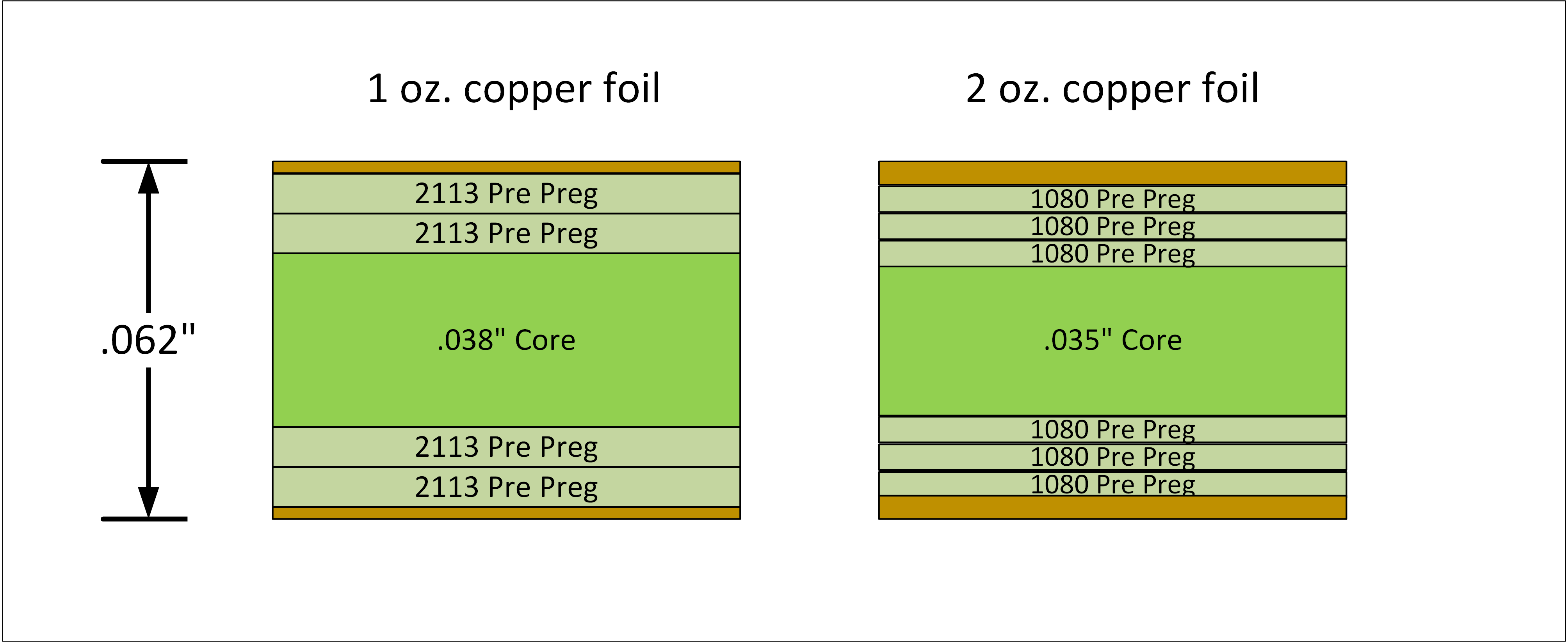
Providing you want to stay with the standard thicknesses, I’ll give you an example of PNC’s standard core thicknesses based off the core copper thickness. Let’s take an .062 and compare the stack-ups. See Figure  below:

Stack-up for an .062 multilayer:
062 thick PCB (002)


Notice to achieve the .062 overall thickness, the core thickness needs to be compensated based on the copper weight of the design. When using 1 oz copper we would use .038 core and .035 core for 2 oz. Also, the amount of pre preg would need to be adjusted as well to get to the thickness required. This is just one example when trying to determine overall thickness of your PCB.

The maximum PCB thickness is usually governed by something called the drill aspect ratio, which is the ratio of a drilled holes depth vs its diameter. When a hole is drilled, the deeper the holes becomes the harder it is to guide the drill accurately (because the drill deflects as it is pushed through the material) until you eventually reach a limit where you can no longer guarantee that the resulting drill hole will be centered in all the pads through the PCB. This is also referred to as drill wander in the PC Board fabrication world.

The aspect ratio for a through hole is the (board thickness) / (drill hole diameter).

Typically, the ratio is limited to approximately 10:1 This means that for a .062” thick board the smallest through-hole drill size is .006” which is the minimum drill size available at PNC. For a .093” thick PCB the smallest drill hole size will be .009” As board thickness increases, more complex via creation techniques such as laser drilled microvias are required to maintain the required pad density under components such as BGAs.

PCB thickness considerations for high speed circuits

One of the assumptions an electrical engineer makes when designing a circuit is that the PCB itself does not contribute any impedance to the circuit. However, in high-speed PCB design the integrity of the signals is definitely affected by the physical characteristics of the PCB.

Unfortunately for the designer the primary sources of parasitic capacitance and inductance of a PCB are affected by board thickness in conflicting ways, forcing the designer to carefully consider the trade-offs.

Vias

PCB vias can introduce both inductance and capacitance to the high-speed circuit. Parasitic inductance and capacitance of a via both increase proportional to board thickness.

Capacitance between layers
The capacitance between traces on different board layers or between traces and the ground plane are inversely proportional to the thickness of the dielectric between them. More space between layers will reduce parasitic capacitance and ensuring that all high-speed signal traces are the same distance from the ground plane will help impedance matching between them.

Crosstalk

Crosstalk between signal traces can be minimized by routing the PCB traces further apart and reducing the dielectric thickness between PCB trace and reference plane.

Mechanical Constraints

A PCB is ultimately a mechanical component of the product and is therefore subject to a variety of mechanical constraints. The PCB or PCBs must fit within the product envelope. This often requires that a PCB be as thin as possible. On the other hand, PCBs are subject to the torqueing forces from cables connected to the board edge and external connections. Preventing board failure during assembly or in use requires a circuit board fabrication thick enough to withstand these forces.

Finally, PCBs in the field are subjected to both vibration and shock. For example, large PCB panels can vibrate in several different modes when subjected to vehicle vibration, causing fatigue and eventual failure of solder joints. The rule of thumb is to get the resonance modes of a PCB to be 10X the input vibration. This requires designing thicker, stiffer PCBS and by careful placement and design of the PCB mounts.

These are the three most important considerations in selecting a PCB thickness. To optimize a PCB design, the PCB designer needs to understand all of these requirements and constrains on the PCB lamination stack-up, and have the flexibility to choose a PCB thickness that balances these often conflicting constraints. The team at PNC can help you design a PCB that meets your needs at a competitive cost and lead time.

Telescope

Ensuring a successful Turnkey PCB Assembly project

There are many detailed factors involved when pursuing the right company for your electronic or PCB assembly needs. These factors can be broken down into two distinct areas, customer communication and supplier contract review. Either the customer or the supplier cannot afford time lost if there is a misunderstanding or lack of data to efficiently and effectively produce a quality product on time. Time spent up front makes for a smooth and efficient transition through the quoting and manufacturing process.

Customer communication

A majority of communications for a request for quote, RFQ’s, in today’s industry are via email. The email needs to contain the required data files and be clear and concise in regard to quantities and delivery dates, along with any details that are not stated on the fabrication/assembly drawings. Since we are talking about Printed Circuit Board Assembly Turnkey projects, let’s break this down further with the required data files for PCB and PCBA.

PCB data files:

1- Fab drawing with build details such as material type, thickness, Copper weight, Tg rating, IPC-A-600 Class, Stack-up, Drill Chart, LPI & silk screen color, Serialization, Panelization array, MIL Spec, final finish and type(RoHs/Non RoHs) etc.
2- Complete set of gerber files.
3- Drill files.
4- IPC-356 Netlist for electrical testing.
5- Read me file for additional information not stated in fabrication drawing or email.

PCB Assembly data files:

1- BOM with manufacturers part number/description and alternates if applicable or DNP’s.
2- Assembly drawing with build details, Solder paste requirements, torque specs, IPC-A-610 Class, DNP’s, serialization, etc.
3- Pick & Place file.
4- ICT or Probe testing if applicable.
5- Functional test procedure if applicable.
6- Read me file additional information not stated in fabrication drawing or email.
If all the required information and data files are complete, we have successfully met the first half of the RFQ process. With this in mind, it’s up to us to compile this information in our contract review process. Let’s take a look at what is processed on our end to complete the RFQ cycle.

Supplier Contract review

All incoming turnkey projects are given an internal number for uniqueness especially for part numbers that has been revised. They are stored in a secure file folder based on two groups of data. ITAR data is stored separately than non-ITAR data. Once the customers data is stored and secure, engineering is notified to start to contract review process for the PCB and PCBA data sets.

Contract review for PCB:

1- Gerber files are imported and overlaid into correct layer structure.
2- Drill files are imported and overlaid against the gerbers.
3- If there is no IPC-356 Net list file, we extract the net from the gerber.
4- The gerbers are ran through a design rule check for manufacturability.
5- Fab drawing is reviewed by engineering for manufacturing capability.
6- If any discrepancies are determined, customer is notified immediately, If no discrepancies, engineering hands off the internal contract review check sheet to customer service.

Contract review for PCB Assembly:

1- BOM is scrubbed to ensure all parts are identified by manufacturer and P/N.
2- BOM parts stock research from approved vendor list.
3- Assembly drawing reviewed by engineering for assembly capability.
4- Pick & Place file review.
5- Review for testing if applicable.
6- If any discrepancies are determined, customer is notified immediately, If no discrepancies, engineering notifies customer service.
7- Quoting team is notified to officially create the quote and send to customer.
Customer communication and supplier contract review is a relatively simple step in order to achieve and ensure a successful assembly turnkey project. Adhering to the steps above can make for a great partnership.

Next Generation Motor Drives

Over the last decade, the semiconductor industry has made great advancements at the component level, especially in power handling capacity, speed and compact size. Due to availability of right power electronics and logic controllers, motor Drives controllers have significantly progressed achieving tighter motion control and increased reliability to different motor types. However Brush-less DC Motors (BLDC) are becoming the preferred choice for low to medium power needs due to its mechanical reliability.

There are many popular electronic products out there using BLDC drives that are not updated to the latest innovations in microprocessor, power electronics and motor control loop algorithms. The reason behind this may be that these products are popular and generating revenue. Unfortunately, these products will not compete with similar newer designs having the latest BLDC drive controller, for many reasons such as: reliability, performance, efficiency, size, weight and cost. Often enough, established OEMs disappear from the market in a blink of eye, due to obsolete products. Over the years we have seen several examples of famous manufacturers in the mobile phone industry parish. BLDC technology is no different, it’s never too late, to upgrade your existing products to ensure your end user trouble free use.

index

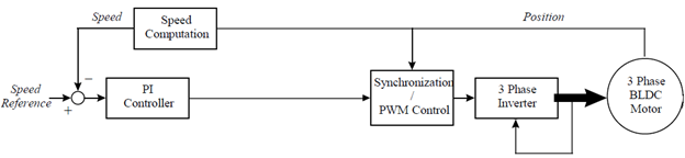
The old methods are based only on speed control loops within the hardware, and specifically dedicated to the motor control chip. Today’s current BLDC motor speed controls play an important role in modern day motor electronics. The control methods are usually divided into two main types, open loop and closed loop. Dual closed-loop speed control is a common control system, with an inner loop for current or torque, while the outer loop is for speed. Dual closed-loop systems provide greater flexibility over Single closed loop systems in various ways, including non-linear control, peak current & bus voltage, deep predictions during acceleration, smart regenerative braking, etc.

index1


Compared with the dedicated motor control chip (analog), the digital control system has the following advantages:

The digital devices have higher reliability, flexibility and stability compared with analog devices.
A digital control system has a higher anti-disturbance ability.
A digital control system could implement more complex control algorithms.
A digital system is more suitable to communicate with top-level system or remote control unit so as to construct a distributed control network.

index3

Digital control systems with dual closed-loop control algorithms can be made independent of motor parameters without changing software or hardware. This allows any OEM the flexibility to switch motor manufacturers, giving them the ultimate freedom of choice. New algorithms can be upgraded within the software controlling the motors at any point in the field with no down-time. If wireless technology is utilized, upgrades or new versions can be downloaded seamlessly as well.

It’s never too late to better your Product to be more reliable or efficient. Do it wisely today, as your Company will benefit from your Customers appreciation of innovative thinking.

This article was written by Sam Sangani Jr., PNC Inc.’s Fellow Design Engineer. you can reach Sam via e-mail at sam@pnconline.com.