Tag Archives: PC Board

PCB FABRICATION SUBSTRATES

PCB FABRICATION SUBSTRATES

What is PCB substrate?

Every home is required to have a solid foundation. A substrate is also required for every printed circuit board. The actual substance that contains the traces and elements is known as the PCB Fabrication substrate. The first step in creating a high-quality PCB is selecting the correct substrate. Structure and shape are required for a PCB. It also requires a platform or canvas on which to place all of its other components. The PCB’s performance is influenced by the substrate’s properties. A stiff substrate, for example, can improve the PCB’s strength and endurance. More design options are available with a flexible substrate.

The usage of a variety of substrates, ranging from solid fiberglass to flexible polymers, is becoming more common as the PCB industry evolves. Fiberglass has traditionally been the most prevalent type of substrate. It’s a low-cost, high-reliability material that gives the PCB a nice, stable foundation.
pcb board
pcb board

 Material of PCB substrate

It’s only reasonable that the materials you choose have an impact on your product’s performance. It’s the same with printed circuit boards, where selecting the correct PCB substrate materials can have a significant impact on the board’s performance, durability, and other characteristics.
printed circuit board

Types of PCB substrate material

Following are the good material that we need for PCB substrate.

1. Copper foil:

PCB substrate materials are critical in defining the board’s endurance and quality. Manufacturers appear to be attempting to go towards fine lines and high density. You may be familiar with the term HDI PCB. This is the abbreviation of High-Density Interconnect Printed Circuit Board. To be classed in the HDI category ten years ago, a board had to have a line space (S) and line width (L) of less than 0.1mm. Today’s standards differ from one industry to the next. S and L on electronic devices are frequently set as low as 60m, and in advanced applications, they can even go as low as 40m. Once a thin copper foil substrate is applied, S and L can reach as low as 30m during circuit design development. The ideal thickness is between 9 and 12 meters.

The issue is that a thin copper-coated laminate can be costly and prone to flaws. It’s the most plausible explanation for why corporations use 18-meter-thick copper foil. However, if S and L are less than 20m, normal thickness copper foil may not be the best option.

pcborard
pcborard
 2. Dielectric Insulating Coatings:

The ability to build up is a key feature of HDI printed circuit boards. There’s a good probability you’ll be able to construct an appropriate circuit if you utilize resin-coated copper (RCC) or combine copper foil lamination with epoxy glass prepreg cloth. MSPA and SAP techniques have also been implemented by the manufacturers. By using an insulating dielectric film lamination with chemical copper plating, the copper conducting plane was created. The fundamental reason we can make acceptable circuits is because of the thin copper plane.

3. High heat protection and dissolution are required:

Electronic devices tend to generate more heat as the trend toward downsizing and high function continues; hence thermal management of electronic devices is becoming increasingly important. Thermal-conducting PCB research and development is one of the solutions to this problem. The main criteria for a PC Board to operate well in terms of heat resistance and dissipation are the substrate’s heat resistance and dissipation capacity. Improvements in thermal-conducting capabilities of PCBs are now being made through epoxy and filler additions; however this only works in a limited category. The most common way is to use IMS or metal core PCBs as a heating component. This system has several advantages over the typical radiator and fan, including a smaller amount and lower cost.

How to Select Substrate Materials for PCBs

You can choose between three distinct types of PCBs:

• Rigid
• Flexible
• Flex-rigid

The most important goal is to select a board that is ideal for your product. Many people strive for compact size and shape while overlooking performance. Polyimide film is a good choice since it is adaptable and can be used in a variety of applications, including black, white, and transparent. It also ensures a low coefficient of thermal expansion while keeping acceptable heat resistance. The Mylar substrate, on the other hand, is extremely flexible and resistant to external conditions. Furthermore, it is reasonably priced, which is why many consumers consider it. Flexible PCBs must attempt to achieve the same degree of frequency and speed performance as regular PCBs. Flexible boards can be made with advanced polyimide substrates and polytetrafluoroethylene.

Flexible boards are used in a variety of industries, including medicine, smartphones, and gadgets. As a result, the market has been implementing innovations in flexible and ultra-thin multi-layer boards (0.2-0.4mm). You can expect flexible boards to achieve speeds of up to 5Gbps at this time, but you’ll need to choose a substrate material with a low Dk/Df. It’s also a good idea to utilize conductors with a thickness of above 100m, as this will aid with current and power handling.

Best PCB substrate type

A substrate and printed wires are the two main components of a PCB (the copper traces). Substrates that divide the layers are required for multi-layer boards. The substrate works as physical support for the circuit components and printed wires, as well as providing electrical insulation between conductive portions. PCB Substrates are non-conducting materials. They act as a laminated electrical insulator between circuits for this purpose. An electrical insulator is a material that does not conduct electricity because its internal electric charge does not flow freely. As a result, plated through holes are used to connect traces on opposite layers on each layer of circuitry.

A substrate and laminate are commonly used as the foundation or base of a printed circuit board (PCB). The performance of the PCB is determined by the type of laminate and substrate used. As a result, choosing the proper types of PCB material for the job is crucial to getting the greatest results. Any PCB design guide should include such features:

 Working
 Durability
 Cost-effectiveness

The material you choose for your PCB can have an impact on its short- and long-term functionality, along with your contractor’s capacity to build it. You can’t blame the contractor if you buy substandard materials and they fail when your contractor tries to make the board. When maximum performance isn’t a must-have feature for a PCB, lightweight polyester material is typically a fine option. As long as lightweight polyester is utilized in conjunction with printed electronics (PE) technology, there are at least two reasons to choose it in these circumstances. Printed electronics with lightweight polyester have these features:

Cost-effective Lightweight polyester produces less waste, necessitates fewer manufacturing steps, and eliminates the need for desalination and purification.

Adaptability Flexible printed circuits (FPCs) are available, but the level of “bendability” that makes them so appealing is costly to accomplish. PE with lightweight polyester maintains flexibility at a far cheaper cost.

Traditional PCBs, on the other hand, is still the top choice for high-performance applications, and the materials used in their construction should be determined by the type of board required. For example:

 Manage frequencies ranging from 500MHz to 2GHz
 Allow for high power and, as a result, high temperatures
 Be “intense” and complicated
 Manage microwave and above-microwave frequencies

The board’s application decides the substrates and laminates to utilize to a considerable extent. There are five types of substrates, each with its own set of features for specialized purposes.

1. FR-4

Fiberglass substrates are comprised of woven fiberglass that has been impregnated with only a flame-retardant substance. The material is rigid and can be drilled, cut, or machined, although tungsten carbide tools are required due to the abrasive nature of the fiberglass. An FR-4 substrate is more resistant to cracking or breaking than an FR-2 substrate and is typically seen in higher-end devices.

2. RF
Low dielectric polymers are employed in RF substrates, which are used in printed circuit boards for high-power radio frequency applications. Despite its low mechanical qualities, the substrate exhibits remarkable electrical performance.

3. FR-2
This extremely low substrate is comprised of impregnated paper, also known as Phenolic, and is simple to the machine over a fiberglass substrate. Flame Resistant is denoted by the letter “FR.” This substrate is commonly encountered in lower-cost consumer devices.

4. Flex
Flex circuits are those that are meant to be very flexible or slightly flexible. As substrates, thin, flexible polymers are used. Although the manufacturing process is more complicated than utilizing rigid substrates, it provides benefits that rigid substrates cannot, such as reducing space by bending the circuit board to fit a specific place or where repetitive action is essential. A low-thermal resistance substrate is required for power electronics. A ceramic core or metalcore substrate has the essential properties to accommodate larger copper tracks and the high electrical currents that these circuit boards require.

Final Thoughts

Every substrate has its uniqueness and you get to know almost every substrate detail in this write-up. Interested to know more about our facilities at PNC? Contact us at sales@pnconline.com

Layouts of SMT Assembly Line

Layouts of SMT Assembly Line

What is an SMT assembly line?

SMT is a technique that is being used to manufacture assembled pcb’s. Many years ago, circuits were large and cumbersome using hard wire and large through hole components, resulting in electrical products that were large and difficult to operate and transport. Comparing to the conventional method, SMT offers the following advantages: high density, good stability, less cost, miniaturization, sound field control, and other features.

For the size of the previously used through hole components to be decreased and modified to be matched with the smaller electronic component, the electronic device must become micro, such as the small component size 0201. Particularly notable are the large-scale and highly integrated circuits. To fulfill the requirements of consumers while also increasing the competitiveness of the market, we must utilize surface mount components for PC Board assembly. As the electronic component becomes smaller, it must become more useful and intelligent as well. As a result, surface mount technology has become more popular in the electronic industry. Furthermore, the standards for SMT are becoming increasingly stringent to fulfill the demands.

Pcb Assembly
Pcb Assembly

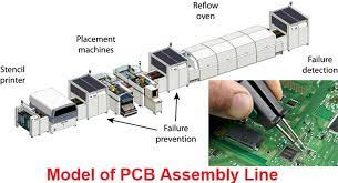
Process of SMT line production

•    Inspecting material using a machine or manual detection.
•    The loader is used to load several printed circuit boards in a row during the setting cycle time.
•    A squeegee is used in screen printing to ensure that the solder is evenly distributed over the panel of the PCB for reflow.
•    SPI inspection is the optical approach used in the examination of solder paste.
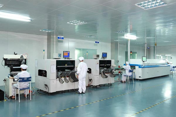
•    Pick and Place machines are used for placing SMT parts in a precise location, which necessitates the use of very fast processing speeds.
•    After the pick and place has completed its task, the AOI machine is used to inspect the quality, particularly for defects.
•    The purpose of a reflow oven is to melt and cool the solder that is situated between the original component and the printed circuit board by international temperature standards. The device and PCB board may then be fused firmly together, resulting in electronic functionality that meets requirements.
•    After completing the reflow oven process, the completed original component and PCB board are subjected to AOI testing.  Its purpose is to check the quality of the solder and assembly of the pasted printed circuit board. It automatically scans the printed circuit board using the camera. A collection of pictures compares the solder junctions that have been verified to the qualifying parameters stored in the database. Then, using image processing, it checks for flaws on the printed circuit board. It indicates the faults via the use of a display or an automated mark for maintenance staff to fix.
•    The completed PCB board is unloaded using an unloader.

Layouts of SMT Lines

Followings are the layouts of SMT lines:
1.    First is the Layout of a single line using a single-rail pick and place machine. This line is a fundamental standard manufacturing line that includes the following machines:

•    The loader is used to load bare PCB boards in a row at the same time during the setting cycle timing.
•     The squeegee, in the solder paste printer, is used to wipe the solder uniformly over the panel of PCB in preparation for the next reflow operation.
•    A conveyor is essentially a device that transports printed circuit boards from one machine to another.
•     When solder is placed between the original component and the PCB board, a single rail reflow oven is utilized to melt and cool the solder.
•    It is necessary to store PCB boards that have exited the reflow oven vertically to prevent damage.
•    The online AOI was used to inspect the completed PCB board after it had been through the reflow oven process.
•    It is necessary to utilize an automated unloader to get the completed PCB board automatically.
2.    A two-to-one line with a single-rail pick and place machine is the layout for this machine. It achieves dual-rail production by merging two independent SMT lines into a single dual-rail line. Because this architecture is intended for a single-lane pick and place machine with just one dual-rail reflow oven available, it achieves dual-rail production. The special machinery that was used in the arrangement included the following:
•    A stacker and magazine loader in one machine.
•    Conveyor for Printed Circuit Boards.
•    Reflow oven with two rails.
3.    Two-to-one line with a dual rail pick and place machine layout is used. In this design, the dual-rail chip mounter and dual-rail reflow oven are combined with three related dual-rail conveyors to provide a seamless connection between the two machines. The benefit of this arrangement is that it allows for the addition of a second SMT assembly line, thereby doubling production capacity. Additionally, the utilization of a PCB Shuttle Conveyor, a dual-rail pick and place machine, and a dual-rail reflow oven resulted in significant space savings.

Get your PCB requirements fulfilled at PNC Inc. Contact us at sales@pnconline.com to get 24/7 support.

HOW DOES SMT ASSEMBLY WORK

HOW DOES SMT ASSEMBLY WORK?

While modern designs for electronics get smaller, more designers depend on the technique of surface mounting. After the 80’s, this technique became famous and hasn’t stopped being the dominant PCB assembly technology for electronics production.

Almost all of the devices in your pocket – either an iPhone xs max or a smartphone – has probably been produced using surface mount technology (SMT). Most of those components in your vehicle or Transportation today have probably been assembled using SMT.

PCB assembly
PCB assembly

What is Surface Mount Technology (SMT)?

Assembling electronics with SMT involves assembling electrical parts using automated equipment that places components on the printed circuit board (PCB).

Manufacturing devices using surface mount technology (SMT) essentially imply electronics assembly using machine tools. In contrast to traditional THT procedures, SMT elements are put directly on top of the PCB rather than soldered to a radial or axial lead. SMT has been the most commonly utilized method in the business when it comes to ethernet interfaces.

Placement and Assembly of Components:

The components to be assembled are inserted into the pick and place feeders or trays. Intelligent software applications guarantee that components are not unintentionally swapped or misloaded during the config file. The SMT pick and place machine then autonomously takes each part from its tray or reel using a pressure pipette and puts it in its proper location on the panel using accurate X-Y cross pre-programming. Our equipment can assemble up to 24,000 parts per hour. Just after SMT assembling has been finished, the PCBs are transported to soldering reflow ovens.

Soldering Components:

The reflow-soldering technique is utilized for series manufacturing orders. This method involves placing PCBs in a nitrogen assisted environment. It is then progressively heated with hot air when the solder paste melts, and the flux vaporizes and attaches the parts to a PC Board. The panels are cooled down after this step.

SMT ASSEMBLY
SMT ASSEMBLY

Solder Paste Usage:

A few of the initial stages in SMT manufacturing is the administration of the solder paste. Solder paste is squeeged through aperature openings in a stainless steel stencil.  Once the squeegee passes over the stencil, the PCB is lowered and travels to the next operation, solder paste inspection, known as SPI. After the solder paste has been verified, the PCB’s move to the SMT pick and place machine.

AOI System in SMT:

AOI visual inspections should be carried out for virtually all manufacturing orders in verifying the quality of completed panels or to capture and rectify an error. The AOI section analyzes each Printed circuit board with multiple cameras and analyzes the look of each circuit to the proper, pre-defined sample image. They will either fix the error or remove the panel from the device to examine it further. The AOI visual management guarantees consistency and precision in the manufacturing process of the SMT assembly.

SMT Components that are not Suitable for Auto Pick & Place:

While most components are placed automatically, others are not installed. This can be for several reasons. Some of them are,

Ø Thermal stress:

Other circuits may be too resistant to thermal and are not perfect materials for soldering reflow temps. These materials must be installed manually to protect them following the usual assembly procedure.

Ø Too light:

Specific components are not substantial enough and, consequently, have a low bulk ratio for conventional soldering automated placing equipment.

Ø Rugged solder joints:

Many components, like connection leads, require a stronger solder joint. Some components are soldered manually to enable this.

This enables rapid examination and repair of components that may be at risk of layout for infringements before the soldering oven is passed.

Surface mount technology benefits:

As with cross-holes, both advantages and drawbacks are included with SMT. Let’s start with some SMT design advantages:

1.   Efficiency:

Thanks to SMT technology, designers can now transform complicated circuits into smaller PCB’s.

In contrast with using the storage on a PCB more efficiently, the SMT board is quicker to increase its overall capacity.

2.   Fewer mistakes:

SMT assembly is very reliant on technology and not so very dependent on people. SMT is a far less error-prone procedure since it’s nearly fully automated.

3.   Cost Accessibility:

These are some of the reasons for the SMT module was to reduce cost. SMT needs far fewer holes in the circuitry. This substantially reduces manufacturing and handling expenses. Furthermore, SMT is much more able to produce large quantities, thereby improving the unit cost.

SMT Disadvantages:

As with other production processes, SMT design has certain drawbacks. The most important is that it needs considerably more eye for detail than a complete construction. Even if the process is substantially automated, your specifications must still be fulfilled to create quality. This is mainly the responsibility of the inventor and the producer of the electronics equipment.

There may also be problems when SMT can be used to put parts on a PCB that works under circumstances that include:

  • Machine stress
  • Ecological stress
  • Stress of temperature

This issue may be addressed by mixing SMT with complete processes to achieve both advantages. That’s correct — on the very same pitch, you may utilize both!

What is the SMT-SMD Difference?

The distinction between SMD & SMT is that SMD relates to the electronic element placed on a Board. SMD is an integrated circuit.

Surface mount technology (SMT) refers in contrast to the way electrical components are placed on a printed circuit board.

SMT refers to Surface Mount Technology and is the complete technology used to place and solder electronic parts on printed circuit boards or PCBs such as resistors, condensers, transistors, electronic components. The devices utilized are also known as surface mounting devices (SMD), surface-mount devices. It should be pointed out that SMT does not have to preserve for constituent pins utilizing holes, and SMD is considerably smaller than by-pass technology.

SMT features:

  • Parts do not have connections or short leads alone;
  • On the same edge of the PCB, the top part of the device and the solder joint;

SMD features:

  • miniaturization;
  • No plumage (flat / short plumage);
  • authoritative Parenting for PCB assembly mounting;

Uses of Surface Mount Technology:

SMT mounting was developed to produce a better, more robust electrical product.

Many typical uses for surface mounting technology are shown if you look around your workplace or home area. Anytime you need a commodity, turn to the surface mount Device structure:

  • Shorter
  • Thinner
  • Faster
  • Most potent

While an SMT assembly is still utilized in some situations or even in specific places aboard.

Summary:

Utilizing the surface mounting technique for electronic engineering, electronic modules are integrated using automated machines which put various elements onto a PCB.

Contrary to typical technological procedures, SMT components are put directly on the surface of the printed circuit board rather than soldering to a lead. Although an SMT device may seem quite complex, it operates extremely fast. The base of the SMT machine utilizes a tiny vacuum head to collect the parts before putting them accurately in the circuit. These devices, known as “pick” and “place” devices, pick up bits from a periodical and position them on a vacuous circuit board. It is important to remember that the correct programming of these devices plays a significant role in efficiency and durability.

HDI Printed Circuit Board

HDI Printed Circuit Board

HDI boards, another of the highest technology in PCBs, also are accessible at Incredible. HDI Panels have blind and hidden visas and typically include MicroVAX of .006mm or below in size. They feature a greater circuit complexity than ordinary circuit boards.

What is HDI PCB?

HDI stands for High-Density Interconnector. Any SATA connector with a greater wire volume per square meter than a regular board is termed HDI circuit board. HDI PCBs feature narrower gaps and outlines, more minor visa and grab pads, and increased connecting pad frequency. It is beneficial in boosting electrochemical characteristics and lowering the shape and volume of the device. HDI PCB is the superior alternative for the supervisor/ and pricey laminated PCBs.

HDI PCB
HDI PCB

The circuit should have different characteristics for high-speed signal electrical demands The thickness of the board should be increased by downsizing and configurations of the electrical components. The board is also highlighted with outstanding high density, thanks to the assembly procedures for leadless, fine pitched packaging, and simultaneous chip connection.

Difference between standard PC Board and HDI PCBs

HDI naturally offered superior system reliability than non-HDI since the use of tiny blind and entered visas reduces all stretching capacities and inductivities. Because there are no gaps, MicroVAX resistance is near the trace frequency. The straying capacitance of a typical passage is substantially larger, resulting in more impedance irregularity than a sensor. The following are some of the main distinctions between HDIs and regular PCBs:

Typical PCBs:

  • Less than HDI
  • Bigger and heavier panels
  • Through-holes
  • Thermal mechanics
  • Higher layer numbers
  • May experience low-pitch performance issues

HDI PCB:

  • Higher square inch component concentration
  • Smaller, thinner, more useful PCBs
  • Blind, concealed, and MicroVAX solution
  • Direct optical drilling
  • Medium access number
  • increased pin count and small pitch compatibility packages

Layout for HDI?

High-density (HDI) interconnection design refers to a series of strategies to design a PCB where trace widths typically decrease around eight miles (0.2 mm). These strategies are meant to guarantee that your plates remain compact, and element count is increased to a greater density of systems into a single panel. Not all circuits need HDI designing approaches for a myriad of purposes, whereas certain parts require HDI approaches for effective routing.

An HDI board needs smaller vias to achieve layer transformations, especially for BGA great devices and more lines per mm2. For exemplary pitch modules, the following common characteristics are included in an HDI structure:

HDI
HDI

Ø Smaller vias:

For layer changeover, HDI boards typically employ microvias or laser-bound, delusional, and stagger vias. Such pathways have a lower refresh rate than usual pathways. Their widths are lower, and their practical depth is consequently limited to employ these Vias using fine-tuning components.

Ø Diluted traces:

The smaller trails used in HDI panels are necessary to link the vias on every layer and the in-pad vias. These smaller traces permit increased trace frequency, the name HDI.

Ø Count of higher layer:

the constructed of non-HDI panels with large layer numbers, but when dealing with high pin frequency electronics, HDI layer numbers may quickly exceed 20 may be more layers.

Ø Lower levels of signal:

For high frequency or high tides, HDI circuits are not utilized. The elevated field strength between adjoining lines causes ESDs, and high tides create an excessive increase in conductive temperature.

Looking at the above criteria and IPC requirements, you may determine whether a board is transitioning to the HDI system, which requires HDI design and routing technology. The current permissible aspect ratio for through-the-hole vias is 8:2 as per IPC-2321A/IPC-2422 regulations (aperture = via detail diameter). This indicates that the lowest drill diameter for a cross hole through a normal thickness of 1,56 mm PCB amounts to 0,197 mm or ~8 miles. As your Via has to be shorter to enable fine pitch parts, certain HDI specialized modules must be used through layouts and smaller traces.

HDI PCB advantages:

The virtual world becomes sophisticated day by day, while the hardware involved becomes much smaller. There are various benefits of HDI PCBs, beginning with greater connectors in smaller regions. As a consequence, boards may be miniaturized in diverse fields.

Your devices are not hefty anymore. They’re smart and attractive. You can operate on your notebook and keep your company going on a trip. You may also view your smartphone’s favorite action film, some quite strong compared to your computers. Or you may connect in and then get into the rhythm with your wireless earbuds. The human race loves technology, and it has become a part of everyone’s life. All electrical equipment was built for mobility at this time. Electronic gadgets for recreation purposes are developed. All this was feasible because the parts and PCBs within the electronic gadgets were miniaturized.

In developing all electrical devices, the PCB sector plays a vital role. Maybe this will be a pacemaker or chipset at a software’s workstation; PCB allowed the creation of critical digital equipment.

1.   Fantastic flexibility:

HDI circuits are appropriate for those who focus on weight, economy, dependability, and efficiency.

2.   Easy installation:

The integration of blind visas and MicroVAX reduces the space need.

3.   Better integrity of signal:

HDI includes technology through inside and blind. This helps to bring the circuits closer together, which reduces the length of the signal route. The HDI feature reduces through stubs and decreases signal distortions, and improves system performance. It enhances the signal integrity considerably owing to shorter signal routes.

4.   Signal Credibility:

Stubs and their impact on signals and data transmission rate reduction

5.   High certainty:

Stacked visas give these panels fantastic protection against harsh environments.

6.   Cost-effective:

The capability of a normal 8-layer PCB may be lowered without losing quality to work in a real HDI board.

Why using HDI:

HDI boards are particularly attractive to portable, mobile, and portable electronics due to their slim, dependable performance and tiny size. These heavier, small molecules and extra transistors interact with the layout of and improve skills to increase the performance of the Printed Circuit Board and the finished result for which it is employed.

Electrical signals require reduced time to travel with equipment closer to one side. The elevated design of HDI panels decreases the signal increases and the capacitance, reducing the impact on surrounding pins and pipes. Additional circuits provide not only an improved user experience but also greater performance.

Focusing on HDI architecture reduces the time and expense of growing prototypes, shortens lead times, and provides a substantial cost advantage.

o   Automotive:

Automobile makers are very attracted by compact PCBs because they can also save room in the car. The merging of technological gadgets to create better driving dynamics was the emphasis of carmakers on future automobiles from firms like Tesla.

o   Medicare:

The HDI PCB influences the medical sector. Medical equipment is frequently HDI since it can integrate into compact devices such as implants, laboratories, and imagery. Medical devices play a key part in illness diagnosis and support life. Ex: defibrillators, patient monitoring equipment.

The inside section of the patients may be viewed, and the correct diagnosis may be obtained using the tiny camera dimensions. The cameras are becoming smaller, yet the quality of the image is not affected. The HDI PCB was developed to enable these advances to be accommodated.

The sensors that have to be placed from equal angles, which some people consider discouraging, have decreased in size with a higher quality of images. Doing a colonoscopy will no longer hurt a lot.

Tablets and smartphones:

All cellphones are ELIC-built HDI PCBs (Each Layer Connectivity). Smaller transportable electronic gadgets are responsible for generating thinner HDI PCBs.

o   Aerospace and military:

HDI is included in secure systems and other critical equipment such as missiles and defensive systems. The HDI PCBs are appropriate for severe and dangerous settings, making them perfect for aircraft and medical operations.

o   Wearable devices:

HDI has become a key consumer player by launching Apple Watch and other accessories such as VR headsets. Digital devices have become popular with the youthful generation because of their outstanding utility.

HDI board types:

A range of vertical goods includes HDI boards, such as missile guidance makers and essential devices and diagnostic devices. The lightweight of HDI panels is also excellent for the aerospace industry and smaller laptops and smartphones.

These are some renowned circuit boards of HDI manufactured.

  • Using surface-to-surface vias
  • Confluence through vias and entered vias
  • Multiple layers of HDI contained through
  • A passive substratum without electronic components
  • Coreless design by using layer sets
  • Alternate coreless buildings by using layer groups

Final Thoughts

HDI circuits are appropriate and preferable for most applications relating to aviation, consumer items, electronic components. Due to its powerful connection of stacked vias, HDI boards with many layers provide greater durability even in intensive environments.

The decrease in pressure gradient creates more room for designers to work, opening up the bare PCB to both edges for design. More closely located smaller components generate greater interfaces, enabling faster communication capability and a significant decrease in bridging delays and loss of signal.

The HDI model enables the 8-layer hollow Printed Circuit Board to be reduced to a 4-layer HDI microplate, with fewer layers capable of providing the same or superior performance. This decrease significantly reduces material prices, making HDI innovation for electronics makers more economic. The higher efficiency of micro HDI PCBs makes them dependable even in demanding settings.

At PNC, you will get your HDI circuits done at an affordable rate. Contact us at sales@pnconline.com.

3D Automatic Optical Inspection (AOI) for PCB Assembly Introduction

The highest demand used in quality management of electronic printed circuit boards (PCBs) and PCB assembly is automatic optical inspections and automated optical inspections (in short, AOI) (PCBA). AOI inspects the electronic assemblies such as PCBs mechanical visual inspection to ensure that the components of PCBs are in the right place and the contacts are correct.

Automated optical inspection (AOI) is an intelligent visual inspection of the production of the printed circuit board, where all catastrophic failures (such as broken components) and quality faults can be scanned automatically by a sensor.

It is widely used in the production phase because it is a way of testing without touch. It ensures the multi-layer circuit boards provide a high degree of durability.

For the following various applications, it is essential:

  • Infringements of line spacing
  • Violation of spacing
  • Copper excess
  • The shortage of pad
  • Short circuits
  • high frequency
PC board
PC board

What does AOI inspect?

AOI is a primary method used to build and test electronic printed circuit boards and PCBs for automatic or automatic optical inspection. Automated optical inspection, AOI allows quick and precise assessment of electronic assemblies and, especially, pcb assembly to ensure that the standard of goods is good and that the object is appropriately and without processing defects.

What is the need for AOI inspection?

Current circuits are much more complex than boards were a few years back, notwithstanding the significant changes that have been developed. With the advent of surface mounting technologies and more size decreases, boards are exceptionally lightweight. Even comparatively ordinary panels have millions of fused joints, and most issues are observed.

This growth in board difficulty also implies that manual examination is currently not a feasible choice. Even if the solution was approved, the inspectors quickly fatigued it, and poor and wrong design was easily overlooked. With great demand, high-quality goods on the market now require very simple, very stable, and fast.

To ensure that the product quality continues to be good, methods are required. AOI is an indispensable instrument within the context of an advanced electronic test plan, ensuring that the expense is held to the lowest possible levels by identifying faults at an early stage of manufacturing.

Benefits over manual visual inspection

PCB devices switch to ultra-thin, lightweight, higher densities, and exemplary size components. The part assembly width of the circuit board has increased, the width and distance of the Printed Circuit Board -line and the pad are decreasing and reaching the micro-level. The manual process of visual examination cannot be achieved. Furthermore, people seem to be tired and emotionally affected, according to the textbook. Inspection equipment is more stable, repeatable, and precise when it comes to machine vision.

Manual visual examination is a vital part of our BES operation. All new boards, either we order from a new supplier or a well-experienced BES company, are visually inspected by us. From solder masks to solder joints, we test all on the floor. Shipping packaging is also evaluated. When we develop our projects, manual visual testing is also helpful throughout the development, from designing to large-scale production. It was the first phase in our identification and repetition of design or manufacturing problems.

  • The usual general information SMT operator will fit well for quick and easy manual visual inspection.
  • Manual visual inspection with high flexibility;
  • The original costs are minimal, and only the initial Labour costs are spent, and high expenses are not available;
  • Preparation is fast.

How can time save done from the visual inspection process?

Visual inspection proves to be a game-changer, with many apps in almost every domain. The company is now moving into manufacturing and production, enabling them to use the power of profound learning and thus have quicker, safer, and superior automation.

  • More quickly

CPU speeds, as calculated in FLOPs and even accurate measurements, result in observations and conclusions, which are done incredibly quickly.

  •  Accurate

An automated machine can standardize the measurement of absolute measurements.

  • Trustworthy

The machine is impartial and programmable as required and without doubt following instructions. It is undoubtedly a result of this technological transition that is moving global producers into different production and productivity levels.

Final Thoughts

AOI is a vital factor in ensuring the accuracy of your completed electronics items is defective and accurate. It gives a shorter timeframe, more efficiencies, and lower prices, which would have increased if reworking was required.

The AOI process provides reliable monitoring and resulting information which enables improved quality control procedures management and the correction of potential issues. The algorithms will monitor the successful and defective PC Board components and record them. Efficiency is also improved from the point of view of process control, organizational integrity, and reporting.

The controls provide search, identification, and measurements or diagnosis for the outgoing product condition. Inspection is an operation. Tasks of supervision have typically been assigned to people. Efforts to simplify industrial inspections to eliminate mistakes and reduce monotony have encountered technical constraints and cost factors of deployment. A prototyping model is an occasional compromise. Reviews have released new study status on manual, hybrid, and automatic inspection.

Perhaps the most critical inspection process is the visual inspection of the parts made. Draw the section and equate the area with the painting visually. For units with several functions, this is particularly relevant. Anything may go wrong, and one of the several production cycles.

During AOI, optical inspection algorithms usually use visual techniques to ensure defects on written platforms. They can identify a range of material removals, such as nodules, scratches, and marks, as well as known dimension faults, such as open circuits, shorts, and solder integrity. They will also spot faulty components, missing components, and parts that have been misplaced. All system is designed to monitor tests conducted by manual operators can be carried out much quicker and more reliably.

How can We (PNC ONLINE) help you in 3D Automatic Optical Inspection?

At PNC, you will get your design checked from two (2) Mirtec MV-6 OMNI machines which itself is high-speed/high-performance 3D AOI MACHINE FIFTEEN MEGAPIXEL CoaXPress Camera Technology. It has an advanced eight-phase Color Lighting System Ten Micron / Pixel Precision Telecentric Compound Lens. It is designed with an Integrated Ten Mega Pixel SIDE-VIEWER® Camera System Precision Closed Loop AC Servo Drive Motor System which is extremely simple to program and operate. It also has 3D Co-Planarity Inspection – Gull Wing Device with an example as shown below:

PCB Assembly
PCB Assembly

We follow all the system parameters and are set up to meet IPC inspection requirements. Get your Automatic Optical Inspection done for your 3D design at PNC. Contact us at sales@pnconline.com