Tag Archives: Printed Circuit Boards

Printed Circuit Board

Printed Circuit Board Heat Sink Features/Functions

Heat management is essential for living on this earth as weather and devices affect buildings, vehicles, and equipment. Thermal management is also necessary for printed circuit boards, as they will get damaged if they can’t dissipate the heat their components generate. Besides, the board also gets hot due to soldering during manufacturing. Hence, heat dissipation methods become mandatory to increase the PCB speed.

Though FR4 is good at heat management, sometimes it is not enough when there is a high-speed circuit board. Likewise, the power supplies also generate heat and you have to install heat sinks and insulators. You must have experienced mechanical engineers to assess the heat flow to create a suitable heat dissipation system.

Printed circuit boards provide current to help devices function, but electronic devices get hot and heat sinks dissipate unnecessary heat. A PCB Manufacturer will use different heat sinks to prevent the overheating of PCB components and their damage, increasing the performance of the board.

Fourier’s law is an important law of heat that determines the heat sink function. When an element gets hot, heat travels from high-temperature areas to a low- temperature surface. The heat transfer occurs in three ways, such as:

  • Conduction
  • Radiation
  • Convention

When two components having different temperatures connect, it results in thermal conduction. In other words, fast molecules collide with slow molecules, resulting in heat transfer from hot components to cool components. PCB has high-temperature components like transistors, so you need to dissipate heat to cooling mediums, like water, air, or it can be oil, or some other element. This heat transfer occurs through conduction and convention.

Types of Heat Sinks

Heat sinks come up in different types as below:

Active Heat Sinks: There is a fan in an active heat sink to provide cooling. Such a heat sink provides great cooling, however, it needs regular maintenance as it is mostly running which affects its condition.

Passive Heat Sink: Passive heat sink is without a fan, so it remains still and needs less maintenance. You can consider it reliable and more effective than an active heat sink.

The shape and design also determine the type of heat sink, including swaged, stamped heat sinks, machining, folded and bonded fin, single fin sink, and forged heat sink.

Factors Affecting a Heat Sink

The main purpose of the heat sink is to exchange heat, so a large part of its surface area should be in contact with the cooling component like air. The quality of the heat sink depends on different factors, including its material, finishing, and certain physical features, like:

  • Air velocity
  • Attachment technique
  • Protrusion type

    Materials That Enhance Heat Sink Function

Manufacturers use specific materials to enhance the function of the heat sink in terms of heat transfer. These materials include:

  • Compounds
  • Conductive tape
  • Thermal paste

These materials are inserted between the surface of the heat sink and the surface of the component that generates heat. Metals having high thermal conductivity are ideal for heat sinks, including aluminum, copper, etc. But, aluminum is common as it is cheaper than others.

What To Consider Regarding Heat Sinks

Many factors affecting heat sink function include length, fin spacing and density, width, airflow, heat resistance, etc.

Which Devices Need Heat Sinks?

Electronic devices with components having poor heat dissipation ability need heat sinks. The devices in this case include multiple integrated circuits, diodes, transistors, switching devices, CPU and graphic processors, and LEDs.

Key Factors of Heat Sink Design

Heat sinks dissipate heat with the help of natural and forced convection, liquid, or radiation. The requirements of thermal management vary, depending upon the applications. Apart from a heat sink design, you have to consider several other factors while designing a thermal management system for a specific device. For like, you have to consider the standards of the component level, heat sink level standards, chassis levels, and requirements for a system level.

Let’s discuss essential factors that you have to consider during heat sink PCB design.

Heat Resistance: Thermal or heat resistance is the sum of multiple resistances occurring to heat flow between a cooling liquid and the die, thermal interference resistance, as well as the resistance between a moving fluid and a heat sink. Thermal resistance is bad for thermally unstable modeling systems.

The Value of Thermal Resistance: It is not precise, instead, it is approximate. It helps evaluate the thermal conductivity of the heat sinks and semiconductors. Heat dissipation depends on heat sink parameters that need proper analysis while designing the heat sink device. Heat sinks can be meshed through a 3D thermal resistance to have a complex system of thermal factors. Different platforms help design heat sink meshes.

Heat Sink Materials:  Generally, copper and aluminum are ideal heat sink materials as described above. These materials are good at conducting heat, especially copper as it also helps absorb heat, resists rust, and resist biofouling, moreover, it is also antimicrobial resistant. Though copper is better than aluminum, it is thick and costly compared to aluminum.

Another material is diamond and its thermal conductivity is also high due to the lattice vibrations it has. Some other materials for thermal applications include copper-tungsten pseudo-alloy, and AlSiCDymalloy.

Size and Shape of Heat Sink:  The shape and the size of the fins also help enhance heat dissipation. You can evaluate various fin shapes through modeling.

Fin Placement or Location: The arrangement of fins in a heat sink affects its cooling quality. Its configuration should be optimized to minimize the resistance of fluid movement, providing maximum air in the heat sink.

Cooling Quality: The cooling quality of the heat sinks has to be high. The aspect ratio of fins should be less to perform well. If the distance of the fin from the heat sink base is more, it will reduce the heat transfer to a cooling medium.

The function of the fins in a heat sink is to absorb heat from the electrical components of a device and sends it to the cooling medium. Besides, you should choose a cooling medium matching a PCB design and device requirements.

Heat Dissipation: Certain factors reduce the heat sink performance like a rough surface and gaps. They cause high resistance to thermal contact, thus affecting heat dissipation. You can reduce such thermal resistance by using thermal interface materials because most resistance-reduction techniques have limitations. You should consider specific things while selecting a thermal interface material, such as contact pressure, the material’s resistivity to current, and the dimensions of the surface gaps.

Attachment Methods: The attachment of the heat sink with PC Board components affects its thermal efficiency. So, you should choose the attachment technique carefully, considering the requirements of a thermal management system in terms of mechanical and thermal properties. Some popular attachment techniques include,

  • Thermal tape
  • Standoff spacers
  • Flat spring clamps

However, these attachment methods don’t end here as there are many others. You would also see m rein the future as engineers continuously update these methods according to new technologies.

By considering the above factors, engineers can design an effective heat dissipation system, including a heat sink.

Frequently Asked Questions

What Is Heat Sink?

The heat sink is a device and a way to manage heat in electronic products. Electronic components like transistors release heat, and you need heat sinks to dissipate heat to cooling mediums, like water, air, or it can be oil and other elements.

Do All Electronic Devices Need Heat Sinks?

Most devices need heat sinks to dissipate heat to cooling components. However, some electronic components have a built-in ability to dissipate heat. Generally, lasers or power transistors can’t transfer heat and need a solution to manage heat. MOSFETs and IGBTs are good examples in this case. So, here you need a heat sink device. 

Can PCB Survive Without Heat Sinks?

PCB components release heat which can damage them, making the electronic device slow. However, it also depends on the PCB materials as some have their heat dissipation property. Mostly you need a cooling system to enhance PCB performance. 

What Are The Types Of Heat Sinks?

The basic types in this case include the active heat sink system and the passive heat sink system. Some other types are also popular, like swaged heat sinks, stamped heat sinks, machining, folded and bonded fin, single-fin sinks, and forged heat sinks. 

Which Factors Influence The Heat Sink Design?

Many factors affect heat sink design, including its material, fin shape, and performance, fin size and location fin configuration, attachment technique of heat sink, and finally the thermal interface.

Final Thoughts

Devices having PCB also have heat sinks because they get hot due to high temperatures caused by different components. Heat sinks are either active or passive. You have to consider a few factors while designing the heat sinks, like its material, fin shape, and performance, fin size and location fin configuration, attachment technique of the heat sink, and finally the thermal interface. Various models help determine the heat sink parameters and geometry to provide a high-level heat transfer.

Would like to know more about the Heat Sink Features and Functions or pcb assembly services? Just Email us at sales@pnconline.com

Metal Core and Metal Black Printed Circuit Board

Printed Circuit Boards are a crucial component of any electronic device, but the materials used to manufacture them can significantly affect the performance and durability of the device. Metal core and metal black PCBs are two types of PCBs that offer numerous benefits over standard FR-4 PCBs. Here, we will explore the advantages of using metal core and metal black PCBs in electronic projects. We will discuss how they can improve their performance and reliability,   as well as their suitability for a variety of applications.

When it comes to a circuit board design, the metal core and metal black printed circuit boards offer a number of advantages over traditional PCBs. These benefits include improved heat dissipation, increased strength, electrical isolation, and reduced electromagnetic interference (EMI).

The use of the metal core and metal black printed circuit boards is a great way to improve the performance of your electronic devices. This type of PC Board provides excellent electrical and thermal conductivity, making them ideal for applications that require more power, speed, and accuracy. Metal core and metal black PCBs are also more resistant to environmental factors, such as temperature changes and corrosion, making them a better option than traditional PCBs.

What Are The Benefits Of Metal Core PCB?

Metal core PCBs are gaining popularity in the electronics industry due to their many advantages over traditional FR-4 and other standard PCBs. Metal core PCBs feature a dielectric layer, which is made from metal instead of a traditional fiberglass-epoxy material used in other PCBs. Such a metal core serves as a heat spreader and helps have better heat dissipation and improved thermal performance. This makes them ideal for applications that require high-level dissipation, and large temperature ranges.

The metal core also allows for a much thinner board than can be achieved with standard PCBs, reducing the overall weight of the assembly and making it easier to integrate into the design. As the metal core increases the rigidity of the board, it reduces the possibility of warping or cracking due to vibration and mechanical shock.

The copper layer used on the MCPCBs is often thicker than on standard boards, providing increased electrical performance as well. The additional copper layer also adds greater protection against EMI (electromagnetic interference), making them ideal for high-frequency and wireless applications.

Another benefit of metal-core PCBs is that they are more reliable than standard PCBs. As the metal core has better thermal conductivity than traditional fiberglass epoxy, it reduces the risk of solder joint failure due to overheating. This means that components are less likely to fail due to excessive heat, resulting in greater reliability.

Overall, the metal core PCBs offer many advantages over traditional PCBs, making them ideal for applications that require high power dissipation, thin boards, or robust performance in harsh environments. While they may cost more upfront than other types of PCBs, the benefits that come with using the MCPCBs often outweigh the costs in terms of improved performance and reliability.

For anyone looking to upgrade an existing project, or build one from scratch, there is never been a better time to consider switching to the metal core. If you’re looking to improve your product’s efficiency and reduce downtime, switching to a metal core PCB, maybe the right move for your next project.

Metal core PCBs are a special type of printed circuit board that uses metal instead of the traditional epoxy resin-based substrate. Metal core PCBs provide many advantages over their traditional counterparts, such as increased heat dissipation and better performance in higher-power applications. However, metal black PCBs offer a slightly different approach.

Metal black PCBs are constructed using metal cores that are plated with a black finish. This black finish helps reduce the emission of electromagnetic interference or EMI that can interfere with sensitive electronic components and impair their performance. Besides, the black finish helps absorb heat, which is beneficial in high-power applications.

The black finish also helps to prevent corrosion in the PCB itself, which can cause premature failure of the PCB over time. Moreover, the black finish increases the electrical resistance of the PCB, which can help protect against the short circuits caused by sudden changes in the voltage.

Finally, the metal black PCB offers an aesthetically pleasing look and a more rugged construction than a traditional printed circuit board. This makes the board ideal for a variety of applications that require superior durability, such as outdoor or industrial environments.

Overall, both metal core and metal black PCBs offer distinct advantages when compared to traditional printed circuit boards. While metal core PCBs provide greater heat dissipation and performance in higher-power applications, metal black PCBs offer superior protection against EMI and corrosion, as well as a more robust design for difficult environments. Ultimately, the choice of which type of PCB to use will depend on the specific requirements of the application.

For instance, if the application requires a higher level of heat dissipation and power output, then metal core PCBs may be preferable. On the other hand, if low levels of EMI emissions and protection against corrosion are desired, then metal black PCBs may be more appropriate. The final decision will ultimately depend on the specific needs of your project.
Which Type Of PCB Is Right For My Project?

When it comes to selecting the right type of PCB for your project, there are a number of factors to consider. One important factor is the type of material used for the PCB. Metal core and metal black PCBs are two popular options for many projects. Each one offers its own unique benefits, so let’s take a closer look at what each has to offer.

Metal core PCBs are constructed with an insulated metal substrate layer sandwiched between two layers of copper. This metal substrate layer helps conduct heat away from the board more efficiently than other PCB types, making it ideal for applications that generate high levels of heat. MCPCBs are also more resistant to temperature fluctuations, which makes them well-suited for automotive and avionics systems that need to perform reliably in changing environments.

Metal black PCBs are a specialized type of MCPCB that offer additional protection against an electrostatic discharge. Such boards contain an integrated layer of insulating polymer that is laminated over the metal core and then coated with a black solder mask. This makes metal core PCBs well-suited for electronic equipment where electromagnetic interference or electrostatic discharge (ESD) could damage the components.

When it comes to choosing the right type of PCB for your project, both MCPCBs and MBPCBs have their advantages and disadvantages. If you need a PCB that can handle high temperatures, then an MCPCB is the right choice. If you need a PCB that provides additional protection against EMI/ESD, then an MBPCB is the better option. Ultimately, it’s important to carefully evaluate your project’s requirements before deciding on which type of PCB is best for your needs.
FAQs
Why DO Manufacturers Us Metal Core And Metal Black PCBs?
When it comes to the design and manufacture of printed circuit boards, there are several advantages to choosing a metal core or metal black PCB. From improved thermal dissipation and electrical conductivity to better environmental protection and durability, these types of boards offer an array of benefits that cannot be achieved with conventional FR4 boards. Not only can metal core and metal black PCBs help reduce costs in the long run, but they can also enable more efficient product designs.

Overall, it’s clear that the benefits of using a metal core or metal black PCB greatly outweigh the costs.

What Is A Metal Core PCB?

Metal core PCB is a special type of printed circuit board that uses metal instead of the traditional epoxy resin-based substrate. Metal core PCBs provide many advantages over their traditional counterparts, such as increased heat dissipation and better performance in higher-power applications. However, metal black PCBs offer a slightly different approach.

What Includes In A Metal Core PCB?

The structure of a metal core PCB has multiple layers, including the circuit, copper, metallic, and dielectric layer, as well as the solder mask.

Wrap Up

In conclusion, metal core and metal black PCBs offer a range of advantages for designers and manufacturers. They provide superior heat dissipation, improved mechanical strength, longer product lifecycles, and improved EMI shielding properties. These advantages can help reduce costs and increase the longevity of the products, leading to improved customer satisfaction and increased profits.

Whether you are looking for increased performance, durability, or functionality, the metal core and metal black PCBs offer an ideal solution. The exceptional benefits these materials provide make them an ideal choice for engineers designing high-end applications.

With their ability to improve product performance while reducing production costs, the metal core and metal black PCBs should be seriously considered when designing a printed circuit board. With so many different varieties available, the sky’s the limit.

Would like to know more about the metal core and metal black PCB or printed circuit board assembly? Email us at sales@pnconline.com

Copper & Epoxy Filled Vias in a PC Board

Printed circuit boards have holes made through drilling to electrically connect various PCB layers. Manufacturers have to fill vias with different materials which are conducive or non-conductive, including copper, epoxy, etc. Via filling helps reduce air or liquid trapping, thus enhancing a PCB’s function. If anything gets trapped in the hole, it would affect the PCB assembly at a high temperature which is essential for soldering without lead.

Via Filling Through Via-In-Pad

The via-in-pad is the latest technology to fill vias, however, it is more costly than the old methods, such as through-hole. HDI boards with micro-vias work better because of their low weight and compact form factor. Such vias reduce the distance between the components, eliminating trace resistance and enhancing conductivity. The via-in-pad technology also helps deal with the BGA issues.

Advantages of Filled Vias

There are many advantages of copper or epoxy-filled vias, such as:

  • Compact board
  • Reduced layer count
  • The BGA pitches get tight
  • Offer a better electrical and thermal conductivity
  • Enhanced routing
  • Thick layers
  • Reduced EMI
  • They provide a short route, bypassing the capacitors in high-frequency PCBs.
  • They help deal with a low inductance

Types Of Via Filling

PC Board Manufacturers fill vias according to PCB requirements. Some common practices of via filling are as below:
Vias Filled With Conductive Materials
Such vias help in signal transfer and also enhance their thermal transfer. Conductive-filled vias have either copper or silver filling to help conduct maximum heat far from PCB components. As copper is a metal, it protects the IC from heat. There are two types of epoxy fillings, such as
Copper Conductive Epoxy: It is better than silver epoxy when it comes to thermal conductivity. Also, the cost of conductive via fill is often very high, like it is 5 times more than the non-conductive filling.
Silver Epoxy: Silver epoxy is a common practice for via fill because it is cheap. However, it is equally good at conducting the current between the inner layers of a PCB and its vias.
Vias Filled With Non-Conductive Materials
The purpose of the filling of the non-conductive via is to protect vias from debris or other elements. It is obvious from the name that such vias can’t conduct heat or electric signals. But, copper plating is still there that conducts heat and current. It differs from traditional vias that have air in the hole that we replace with a filling material. The non-conductive filling also enhances the structure of the copper pad and covers vias in a via-in-pad technology.
Make sure the CTE value of via filling is compatible with the laminate to prevent stress fractures. The stress occurs because of expansion or contraction, as the filling material gets hot and expands faster than the surrounding laminate. So an unequal expansion can damage the area between the hole’s wall and the pad. The expansion of conductive materials can affect the process of reflow soldering.


Shut-Filled Vias
There is another technique of filling vias known as a copper-plated shut filling, however, a few printed circuit board manufacturers practice it. This method goes well with both through-hole and micro-vias.
Some manufacturers can plate shut the through-hole vias which are 12 mils in diameter. Factors like air or fluid accumulation in the holes don’t matter in this case. The plated shut-via filling is 10 times more in thermal conductivity than other filling methods. Hence, you can consider it a logical and effective way of heat dissipation. In general, the copper-shut via is ideal where the aspect ratio is 10:1 or the diameter of the vias is lower than 8mils.
The plate shut technique makes micro-vias more reliable than filling them with a non-conductive material and plating it over. You can have a solid core by filling vias. The plate-shut vias help have a flat surface that you can plate. Moreover, it prevents solder from leaking during pcb assembly, eliminating the solder joint issues. Hence, the plate shut makes assembly more reliable than other via filling technologies.
However, you can’t have plate-shut vias in certain circumstances, such as:

  • The filling material is thin and can’t bear the polarization, as it can tear down.
  • In the case of wrap plating, copper builds up on the terminating surface, making the process hard for fine lines or spaces.
  • Teflon or PTFE materials might distort.

Which One Is Better-Conductive Or Non-Conductive Via Fill

However, conductive epoxy is also available for PCBs having a high amount of current and heat passing vias.
In the case of via-in-pad with through plating and epoxy ink filling (conductive or non-conductive), the epoxy ink goes through polarization to develop a flat surface. Besides, it is filled through plating.
The process of via filling makes CTE stable, keeping out the plating bath solution that affects the board.

What Happens With Unfilled Vias

The BGA balls and the printed circuit board will not have any connection if the via-in-pad is not filled. If the BGA pad has vias, you will have to fill and plate over them. When the vias are between the pads, you can have dams on the solder mask to avoid the solder pastes mitigation.
However, another way is to cover the via with a solder mask to have additional protection when there are thin solder mask dams. Even if you cap vias with the solder mask, the paste can’t stop from spreading on the tracks into vias, thus affecting the mechanical and electrical connection.

What Are PCB Vias

Printed circuit boards have different layers that need electrical connection and vias provide it. So, via is a tiny hole drilled in the PCB laminates, crossing the adjacent layers. Vias are internally covered with copper in different ways. It helps pass current which is essential to run a device.
How many layers the via should cross, depends on the PCB application. Like, it can cross one to two external layers or one or multiple internal layers. Sometimes vias cross all the PCB layers.
Some vias also don’t contribute to the electrical connection but dissipate heat, so we call them thermal vias.

Via Types

There are different types of vias that manufacturers practice according to the PCB application needs. Such as blind vias, buries bias, through-hole vias, and micro-vias. Micro-vias are further divided into blind micro-vias, stacked micro-vias, and staggered micro-vias.
Hence, vias play a great role in a Printed Circuit Board, eventually affecting the function of the device having that PCB. You can hire a good PCB designer and manufacturing company for this purpose. Make sure to have a thorough research in this case to select the best service.

Frequently Asked Questions

Why PCB Vias Need Filling?
Via filling helps reduce air or liquid trapping and enhances a PCB’s function. If holes get clogged or have air, it would affect the SMT assembly at a high temperature.
What Is Conductive Via Fill?
Via filled with a conductive material helps pass current and heat through different PCB parts. Conductive-filled vias have either copper or silver filling to help conduct maximum heat far from PCB components.
What Is Non-Conductive Via Fill?
The reason behind creating the non-conductive via filling is to protect vias from debris or other elements. The name depicts that such vias can’t conduct heat or electric signals. But, copper plating is still there that conducts heat and current.
What If I Leave Via Unfilled?
When the via is not filled, the BGA balls and the printed circuit board will not have any connection. Besides, it will get contaminated, blocking the passage and signal flow.
What Is A Shut-Filled Via?

The shut-filled via is a logical and effective way of heat dissipation. In other words, the copper-shut via is suitable where the aspect ratio is 10:1, or the diameter of the vias is lower than 8mils.
How To Select The Type Of Via Fill Material?
The application of the PCB and its requirements determine the type of via fill you should have. Besides, your budget also matters while selecting the filling material and technology as described above.

Final Thoughts

Printed circuit boards help run different devices by providing them with current, so they have to be perfect t in all ways. Vias are important for a PCB because
Via filling helps have a compact PCB, minimum layers, tight BGA pitch, enhanced electrical and thermal conductivity, better routing, thick layers, less EMI issues, helps cope with low induction and offers a small route and bypass capacitors the high-frequency PCBs. There are two types of epoxy fillings of which the copper-conductive epoxy is better than silver epoxy when it comes to thermal conductivity. Also, the cost of the conductive via filling is 5 times more than the cost of the non-conductive filling.
Silver epoxy is a common practice for via filling because it is cheap. However, it is equally good at conducting the current between the inner layers of a PCB and its vias.
Would like to know more about Copper and Epoxy Filled Vias in PCB or printed circuit board assembly? Email us at sales@pnconline.com

Acceptability Criteria of Printed Circuit Board, what standard do you use?

banner-131001

As a printed circuit board manufacturer, PNC Inc., Nutley, NJ, our criteria of acceptability during the inspection process is determined by IPC–A–600. The scope of this document describes the acceptable and non-conforming conditions of a bare boards either externally or internally during the final inspection process. The inspection criteria is then broken down into three classifications of acceptability, Class I, Class II and Class III. Each class’s acceptance criteria is then again broken down into three areas, target condition, acceptable, and nonconforming for the imperfections in question.

At times there can be a disconnect or confusion between the end-user and the manufacturer in terms of acceptability criteria. Why? Is the PC board manufacturer shipping inferior product, or not interpreting the IPC standard incorrectly? Does the end-user use a standard for acceptability during incoming inspection, such as IPC-6012? These are only a couple of questions why there may be a disconnect in determining the acceptance or nonconformance of a bare rigid board.

The intention of this blog is to help inform and decipher the IPC–A–600 acceptance criteria for a bare printed circuit board. Over the next few months, I will break down imperfections with pictorials, and explanations of the acceptance, or nonconformance for a particular imperfection. I will start with the most common defects seen in the manufacturing process of a PC Board.

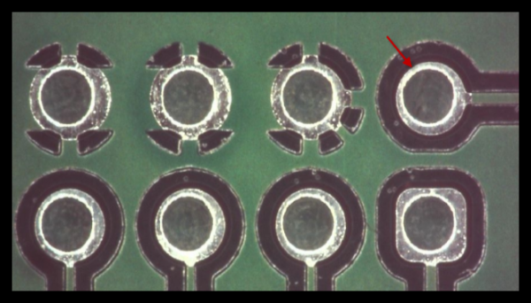
Today, I’d like to look at one of the most common occurrences, external annular ring of supported holes. The condition in question is where the drill in the plated through hole appears to be off center in the pad, as seen in figure 1 below. This occurrence happens because of manufacturing tole rance build ups through the process. The two main contributors are Drilling and Primary Imaging.

Annular-Ring-Break-out

Figure 1

The combined tolerance between the two processes for most PC Board Manufacturers can be +/- .003 for positional accuracy. Typically most Drilling Machines have a positional accuracy of anywhere from .0005” – .001”, whereas primary imaging photo tool registration can be out as much as .003” due to film stretch or shrinkage. In knowing that there are manufacturing tolerances involved, let’s look at the IPC rule for this condition.

According to IPC-A-600, Acceptability of Printed Circuit Boards, we need to determine the minimum annular ring of the supported hole. This can be found in section 2.10.3 External Annular Ring-Supported Holes, as seen in Figure 2103a, since there is no break out. As you can see the target condition is where the hole is centered within the land.

IPC-Class-1-2-3-Target-Contition

The ruling criteria can also be found in Table 3-5 Minimum Annular Ring from IPC-6012B. For the holes in question from Figure 1, the inspection process used Class II as their criteria.

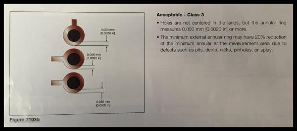
After viewing the customer’s original Gerber data, we find that the annular ring is specified at .009 “. Our findings at the narrowest point of the annular ring measured was .006” on the board. We know that it does not meet the Target condition for Class II per IPC, so we’ll look at the acceptable condition from Figure 2103b.

IPC-Class-1-2-3-Target-Acceptance-Class-3

In this case, Class III is the only acceptable criteria for this condition which states, “Holes not centered in the lands, but the annular ring measures .050 mm or .002” or more. Also during the observation, there were no defects such as pits, dents, nicks, pinholes or Splay, so we do not use the 20% rule for this condition. Knowing that we have more than .002” of annular ring remaining, this condition passes the inspection process per IPC-A-600 section 2.10.3.

I realize to most of you that this is very elementary, and the rule is straight forward. In saying that, we find ourselves defending the IPC rules with individuals whom are unaware of IPC-A-600 and/or IPC-6012 standards. Over the past 20+ years in this business, I have seen great strides in companies having their employees educated and/or certified to IPC standards. I can only hope the trend continues.

request-for-more-info-button1