Tag Archives: PCB manufacturer

PCB Design, Selecting the Right PCB Trace Widths?

Every PCB designer has a series of decisions to make PCB Design as they translate an abstract schematic into a functional, reliable, and manufacturable PCB assembly. Placing the components on the    PCB is usually the first step, connecting those components with copper conductors to create the circuit is the next.  To connect the components, the layout designer must interpret the circuit netlist and turn that netlist into actual copper traces, subject to constraints of both manufacturing technology and the laws of physics.  One of the most important considerations for the designer is the appropriate trace width for each of those connections. The width of each trace determines both the real-world performance of the circuit and the overall size and number of layers of the PCB.

To balance circuit performance and PCB size, the designer needs to balance four considerations:

  • The manufacturer’s minimum trace width and spacing
  • The size and pitch of the component pads that the trace will connect
  • The amount of current flowing through the trace
  • Whether the trace is part of a controlled impedance circuit

Minimum Trace Width and Spacing

The manufacturer’s minimum trace width and trace spacing will define the smallest trace width that can be used for all signal traces that do not carry significant current or have impedance constraints.  The minimum trace width is typically used as the default for the layout, since using the minimum trace width will result in the smallest possible PCB and the most flexibility in routing.

For a standard Printed Circuit Board, fabrication minimum trace widths/spacing is typically 5 mil (.127mm). PNC’s High Density Interconnect (HDI) PCB trace width/spacing can be as narrow as 3 mils (.076mm)

Trace Width vs Pad Width

Another consideration when selecting trace widths is that the trace should be smaller or equal to the pad width. For the most part, if working with the minimum trace widths, this will not be an issue, however, care must be taken when laying out the traces and pads for high current applications.

High Current Traces

Once a designer has placed the components in the layout, they will often focus next on creating the power and ground traces to the active components.  This is because the current carrying traces need to be appropriately sized and routed.   Signal traces, which are typically at the minimum trace width, can be more easily routed around the larger power traces.

Copper PCB traces, like any conductor, have an internal resistance that is proportional to the conductor length, and inversely proportional to its cross-sectional area. Since the copper on a layer is of a uniform thickness, the width of the trace determines its cross-sectional area.  There will be both a voltage drop along the trace as well as heating of the trace due to the power dissipation.  If a PC Board trace is not sized appropriately to carry the current required by the circuit, the trace can fail due to overheating, or the high voltage drop along the trace can cause intermittent circuit problems as the current and thus the voltage drop in the trace varies over time.

Designers often create an internal copperlayer with multiple buses of various voltages.  Since that layer consists only of power busses, the buses can be quite wide.  The designer will then connect the individual components to the bus using vias rising to the component’s power pins.  A bus based design reduces voltage drop at far from the power supply while reducing the width of the short connector trace to the same size as the component pin pad.

In the days before the internet and sophisticated PCB layout software,  designers would use the pages of current vs trace width tables  in IPC 2152 “Standard for Determining Current Carrying Capacity in Printed Board Design”  Now there are online calculators  based on those tables that take in to consideration all of the factors involved in determining the appropriate trace width for a specific current and allowable temperature rise of the trace due to the power dissipation. Many full featured Printed Circuit Board layout applications have the calculations embedded in their design rules.

If a PCB is intended for high power applications such as motor control or an LED power supply, a copper layer thicker than the typical 1 oz can be used but note that it is difficult to etch fine traces and pads in thicker copper.  Make sure to check with the PCB fabricator about their capabilities. PNC has experience with thick copper layers and can provide advice to the designer about what is possible.

Controlling Trace Impedance

The last consideration in selecting trace widths is the impedance of the trace, which becomes a factor in high frequency signals such asDDR busses, video such as HDMI, and high speed serial communication like USB and Gigabit Ethernet. At these high frequencies, not only the trace resistance, but the capacitance and inductance of the trace become significant factors.

Designing controlled impedance (CI) circuits is beyond the scope of this post, because designing a controlled impedance circuit requires taking into account the dielectric constant of the PCB, the length and routing of the trace in addition to the width of the trace.  However, trace width is one of the most easily controlled elements of impedance controlled circuits,so the trace width on individual controlled impedance circuits may be different from the width of other low frequency signal traces, and those traces may be finetuned after the prototype PCBs are tested.

The design of controlled impedance circuits is described in detail in IPC-2141A “Design Guide for High-Speed Controlled Impedance Circuit Boards”, and many of the formulas are available in online calculators or as options in PCB layout applications. When designing high speed circuits, it also pays to work with a PCB manufacturer like PNC that has expertise in fabricating PCBs with precise and consistent dielectric properties.

Schedule a Design Review with your PCBA manufacturer

 The designers at PNC have experience with both high power and high-frequency RF and microwave PCB layout designs.  Because they work closely with the manufacturing team, they know what is possible to achieve with the thick copper layers used in today’s compact LED and motor controllers,  and they know what it takes to maintain consistent dielectric properties in the substrates, needed for predictable RF performance. Let them help you with your design.

Power Electronics: The Hidden Technology

In the last decade of 21st century, power electronics has seen a tremendous amount of growth due to smaller and accurate designs working at the heart of each and every electronic device, machine, appliance or system. The current arena of power electronics is dominated by providing the low noise accurate supply voltage rails and huge power handling capacity at higher efficiency in small factor.
Power electronics in layman terms is defined as the high power circuit design converting one level into different level of electrical energy. Power systems in current decade vary from range of mW (cellular mobile phones) to hundreds of MW. In the last few decades conversion of electrical energy has been done with the dissipative method where most of the energy is dissipated in the form of heat. These types of techniques use normally bulky passive components and huge heat sinks. The usage of huge heat sinks is due to huge amount of power loss and very low efficiency of previous design.

1

According to the latest surveys/research, currently 40% of the world power/energy are met with the usage of electrical systems, with more advancements in the field of renewable resources, the percentage will be going to shoot up to nearly 70-80% in the coming decade by 2025.The efficiency of power equipment varies from 90% (small design) to 95-98% (big complicated design models). Due to rapid advancements in the field of technology, the cost of the circuit and size is reducing at a faster rate and providing more efficiency as compared to the previous possible designs.

Challenges in Designing Power Electronics

The major challenges in the field of power electronics are cost, reliability, parasitic losses and electromagnetic interference. Areas like aerospace industries, automation and robotics industries has posted the biggest problems in front of power engineers because in order to fulfill the safety requirements. The safety requirement is the most difficult and unsolvable challenge in many fields involving power electronics devices.

The old technology of linear dissipative regulator is reliable as compared to newer regulators since new regulators used the bulky capacitors and lesser amount of shielding in the circuit. If due to some fault, larger supply is fed to the circuit then it will suddenly increase the current in the design which will lead to damaging and even burning of the complete circuit.

2

Even the latest MOSFETS or transistors, available in the market comes with very low power wattage i.e. 0.5 W or 1W (at max) in order to provide the cost effectiveness but this make the circuit more prone to damage since even small deviation from the expected behavior can lead to damaging the complete circuit. Ex- observed in the latest gadgets like LED TV’s, Mobile phone (since in order to provide cheaper designs, they are using the devices at the bottle neck of their limits).

3

Electromagnetic Interference in layman terms is defined as the amount of noise/disturbance produced by a power circuit due to change in one of electromagnetic radiation or induction. EMI must be kept in safe level to ensure the reliable operation for the given design.

Issue: Power supplies generate lot of noise in the circuit due to switching current at high operating frequency and most dependent customer being MOSFET for the same. Due to MOSFET, the switching speed is very high varying from 200 KHz to 100 MHz range. The generated EMI due to noise can be characterized as Differential and Common Mode Input

  • Differential Mode Input–It basically consists of in and out of flowing current through the power supply by the path going from power lead to the source. It is the dominated in lower frequency range i.e. less than 5 MHz
  • Common Mode Input – – It basically consists of in and out of flowing current through the power supply by the path going from power lead to the source through the lowest impedance path i.e. ground. It is the dominated in higher frequency range i.e. greater than 5 MHz


Minimizing EMI


  • Bypassing – Bypassing is one of the most effective and cheapest method to tackle this problem. Used for reducing high switching current in the case of MOSFET with the help of large and bulky capacitor.
  • Decoupling –Decoupling refers to isolation of two circuits with the help of a common line. It is implemented using low pass filters.
  • Layout –Increase the distance between VDD and ground plane at the time of chip layout in order to reduce the EMI, reducing the inductor can also provide minimizing the EMI.
  • Shields –Reducing the energy requirement from DC-DC supply by putting a metallic shield outside the power supply.

The single biggest failure for any network/system is power supply which major comprises of the below listed factors

  • Internal supply failure- The Internal Supply failure issue arises in the case of ill-handling the devices but mostly to prevent this problem, there is an automatic shut off system inbuilt in our Laptops and other electronic devices.
  • Voltage Irregularities– Most commonly consists of high voltage spikes, surges and delay in either input paths which switches the logic value.
  • Outraged Power –Mostly external power failures due to change in supply voltage from the plugs can cause outraged power. This will happen for short span of time varying for some seconds to minutes.

Motor Control EMI: AC Mains Conducted Emission

We do not want our product to come back from testing to find that we have failed electromagnetic interference (EMI) or conducted emissions (CE) exams. Furthermore, we do not want these noise sources to degrade our products performance, so we need to understand the mechanisms of this noise and how to minimize it.

One of the most common failures is, AC mains conducted emission testing which is listed as IEC 61326-1:2005, Ed. 1 section 7 (CiSPR11:2003). The purpose of the conducted emissions test is to measure noise currents that exit the products ac power cord to be sure the currents are within the regulated limits. The most efficient method for the reduction of conducted emissions is to reduce them at their sources. In this section we will discuss the source of conducted Emission on AC mains and how we can minimize the emissions. In following section we will focus on workarounds for the system has failed pass the AC mains conducted emission test.


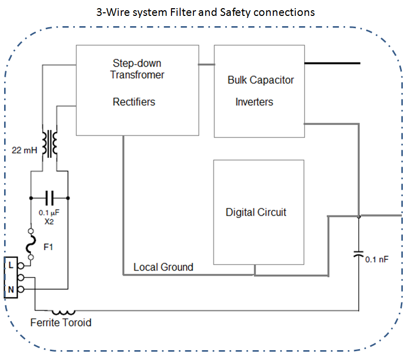
3 Wire system filer and safety connections

Rectifiers:

Fast recovery diodes snap off sharply and generate high frequency noise compared to slow recovery diodes. In order to reduce this undesirable noise generated in the turnoff of the diode, snubber circuits are generally placed in parallel with the diodes. The snubber circuit consists of a resistor in series with a capacitor that acts as a path to discharge the charge stored at the diode junction when the diode turns off. This tends to smooth the diode current waveform, thereby reducing high frequency spectral content. The high frequency current will circulate through the snubber circuit where the leads need be kept short and the elements placed very close to the diode. In doing this, you will reduce the current loop area and the emissions will be radiated from the loop.


Transformer:

Winding the coils on top of each other introduces a parasitic capacitance between the primary and secondary. This primary-to-secondary capacitance can introduce an undesired coupling that allows noise on the secondary side to be more easily coupled to the primary side. Once the noise is present on primary side, it passes out through the power cord and is measured as a conducted emission by the LISN, unless the power supply is inserted between the power cord and transformer. The efficiency of this coupling, due to the parasitic primary-secondary capacitance increases at higher frequencies. In order to reduce this coupling, there is need for a metallic shield between the primary and secondary coils. This is referred to as a Faraday shield. This shield should be connected to the primary side reference or neutral.


Switching devices:

Primary current begins to flow when a MOSFET(s) is turned on. The transformer primary current ramping to a peak value is determined by input voltage, motor phase inductance, switching frequency and duty cycle. This trapezoidal (or triangular) current waveform is characterized in the frequency domain by a spectrum at the switching frequency. The harmonics are determined by the relative squareness of the waveform and causes the primarily differential mode emission currents to circulate between the AC mains and the power supply input. This current waveform can also create common mode emissions, due to radiated magnetic fields when the current path defined on the PC board layout encircles a large physical area.


The spectral content of the noise that is produced by switching is directly dependent on the rise and fall times of pulses. The slow (high) rise and fall times are desirable from the standpoint of EMC. This causes the MOSFET to spend more time in its active region, which increases its power dissipation, therefore is an undesirable result from the standpoint of thermal consideration. Concurrently, there is an apparent tradeoff between reduction of noise spectral content that will contribute to conducted emissions and the thermal heating of the switching element and related efficiency of the switcher.


Wire Harness and System connections:

Noise current sources appear between live and neutral connections without reference to the earth connection. In circuits with a switching power supply or motor control, the RF emissions are dominated by interference developed across the DC link to the switching devices. Although there will be a bulk capacitor, the high di/dt through this capacitor will generate voltages at the harmonics of the switching frequency across its equivalent series impedance.


The coupling is dominated by the inter-winding capacitance of the isolating transformer, stator-rotor of the motor and system to the chassis. These capacitances are referred to earth, either directly or via the enclosure if this is conductive. A well shielded enclosure will minimize “leakage” of this capacitive coupling and hence reduced conducted emissions. Ideal connections for 2-wire and 3-wire system are shown in figure xx and xx.

2 Wire system filer and safety connections.bmp

<br\>


This article was written by Sam Sangani Jr., PNC Inc.’s Fellow Design Engineer. For additional information related to this or any other topic, you can reach Sam via e-mail at sam@pnconline.com.