Tag Archives: circuit board assembly

Improving Speed by PCB Routing Techniques in PCB Layout

PNC-main-mid2

There has been immense development in physical design aspects of designing with the advent of CAD Tools. It’s not that long ago, that we were hand taping on multiple layers of mylar at 2:1, 4:1 and even 8:1, and then having to shoot the artwork with a camera to reduce the film to 1:1. The power of today’s CAD tools can maximize your time whether it be circuit design, circuit simulation, PCB design, or system-level simulation of PCB Layout. In turn, Complex designs can be optimized quicker and more efficiently.

We know that copper traces are used as interconnects or bridges between two unconnected elements of the circuit. The length & shape of these interconnects play an important role in high speed design, since each interconnect is modeled as a combination of resistance, inductance and capacitance, which can in turn change the value of impedance. Taking this into consideration, we try to model PCB Routing Techniques in a more algorithmic and efficient way to improve the speed of the design.

The most challenging task for the designer is the placement of the components in order to minimize the usage of wire and chip area. The design starts with placing the important components of the circuit in terms of design and the entire board to reduce the routing constraints. Finalizing the key elements specific locations (critical components) and routing paths helps in analyzing the critical path and operating frequency of the circuit design. After Placement, particularly for routing a wide variety of analog and digital signals, with varying voltages and currents, ranging from dc to high frequency (GHz), the utmost importance is keeping signals from interfering with one another. The Zero potential planes help in providing a common reference point for devices as well as helping device shielding in order to compensate for any extra amount of current. In the case where signal isolation is required, we need to concentrate on the physical distance between the signal traces.

Major Routing key points

  • Distance between two interconnects must be minimized for particular path.
  • There should be no sharp bends, (90 Deg.) in the track design.
  • Tracks should exit from the center of a connection point, avoiding other interconnects and pads in order to have a high speed and error free design.
  • Do not place via under component.


Proper and Bad Routing Examples

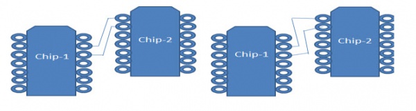
Image: Proper angle routing (left) and bad routing (right)

Reduction in long traces on adjacent layers to prevent capacitive coupling.

  • Reduction in long parallel runs and close proximity of signal traces in order to reduce or eliminate inductive coupling (practically impossible) in a design.
  • Signal traces requiring high isolation should be routed on separate layers and if not possible, orthogonal routing can be done. Orthogonal routing will help in minimizing the capacitive coupling which will lead to the shielding effect by the ground or zero potential.


Automated Routing Techniques can be used for increasing speed

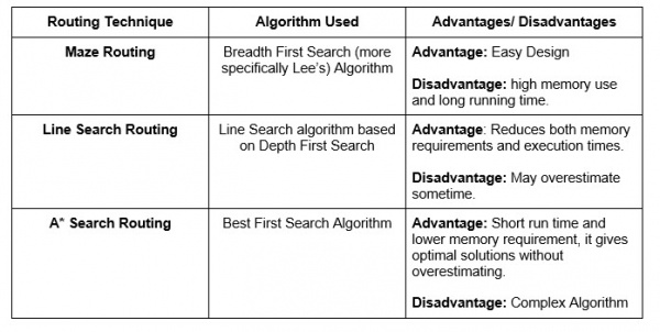
Auto routing within a Design exhausts all the possible implementations of the given possible design and helps to improve the performance, reliability and cost of the circuit design. This innovation is referred to as Electronic Design Automation. The technology has advanced with usage of Artificial intelligence and neural based technology. Automated routers are mainly used when you have a complex board with little routing space. Advanced automated routers allow you to specify exactly how you electrically want to layout the most important tracks. Below is the list of general purpose routing techniques and algorithms (These are algorithm models related to CAD Routing tools) , apart from this there are special routing techniques for power and clock like H-clock tree synthesis.
 

Example of High Speed PCB Routing

Example of High Speed PCB Routing Technique
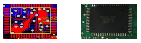
 

Top Layer PCB Design and Final Chip Implementation

Top Layer PCB Design and Final Chip Implementation


The left hand side of the above diagram shows the top view implementation of a PCB design. Due to the simplicity of this design, we can mount all the circuit components on the top layer. The above design will help in eliminating the signal trace which ensures the best possible speed and design of the circuit. The key points in this PCB design is the reduced delay time because the separation of larger bypass caps are placed farther away with ferrite Chips for HF isolation of currents and multiple via which reduces the delay path in the circuit.

request-for-more-info-button1

Grounding in Printed Circuit Board Design

PNC-main-mid2

As we advance into the future, we want everything to be faster, cheaper, compact and durable. Everything around us is electrical. Moore’s law predicted that numbers of transistors per square inch of Printed Circuit Board will double every 2 years and it’s been true too date. Well theoretically it sounds good. But implementing new products with the above requirement comes with a cost. In order to reduce the unit cost of the design, due to noise. Various techniques have been developed in the past few decades to reduce noise in the circuits as the number of components increases and the available size decreases. Design techniques include proper grounding, decoupling, routing and signal multiplexing.

Grounding at PCB level can be in implemented as single point ground. As the name suggests a single point ground is where the complete circuit residing on the PCB has a single ground. This technique is developed by using a ground plane. Ground plane is defined as a highly conductive electrical surface which will be used as a system ground. In printed circuit boards, it is referred to as a large conducting surface of copper foil on either side of the PCB. It is connected to the power supply ground terminal and thus it serves as a return path for current from different components on the board .The fact that a large surface area of highly conductive metal, like copper, has a very low impedance which forms the basis of this method.

Ground plane is laid on the PCB, such that it covers the maximum area which is not occupied by circuitry itself. In multilayer PCB’s, it is often a separate layer covering the entire board. This makes the circuit design easy to implement, thus further allowing the designer to ground any component or subpart of a circuit without adding additional traces. The large area of copper which provides a very low impedance path conducts the large currents originating from other components/subparts without significant voltage drops. This ensures that the ground connection of all the components is at the same reference potential.

request-for-more-info-button1

Benefits of grounding in PCB are:

  • Reducing electrical noise
  • Reduce interference being coupled from one part of the circuit to another.
  • Reducing crosstalk between adjacent circuit traces.

1) Noise reduction:

When circuits switch states, large current flows from the active devices through the ground. If the power supply and ground traces have noticeable impedance, then the voltage drop across them may create noise voltage that would disturb other parts of the circuit. The large conducting area of the ground plane has much lower impedance than a circuit trace, so the current causes less disturbance.

2) Interference & Crosstalk reduction:

When two traces are placed too close to each other, an electrical signal in one can be coupled into the other. This is due to electromagnetic induction caused by the linking of magnetic field lines from one trace to other. This phenomenon is known as crosstalk. When a ground plane layer is present underneath the circuit in the PCB, it acts as a transmission line for the trace. Thus the direction of current flowing through the ground plane is opposite to the direction of current flowing through the circuit trace. This cancels most of the electromagnetic fields and consequently reduces crosstalk.

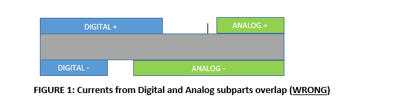
Many of the present day circuits consist of both Analog and Digital subparts. To avoid current from one subpart to affect the other subpart, ground planes are split and then connected by a thin trace. The thin trace has low enough impedance to keep the two sides very close to the same potential while keeping the ground currents of one side from coupling into the other side, completing a ground loop.

11

21

Thus grounding in PCB can significantly improve the circuit/chip performance. No extra area is added to the chip as leftover areas are used. This method doesn’t add too much of cost to the initial design which makes it readily acceptable at industry level.

Types of single ground connection:

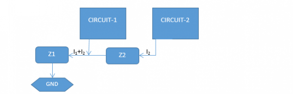
    • Series Ground Connection:

31

    • Parallel Ground Connection

41

Terry

Power Electronics: The Hidden Technology

In the last decade of 21st century, power electronics has seen a tremendous amount of growth due to smaller and accurate designs working at the heart of each and every electronic device, machine, appliance or system. The current arena of power electronics is dominated by providing the low noise accurate supply voltage rails and huge power handling capacity at higher efficiency in small factor.
Power electronics in layman terms is defined as the high power circuit design converting one level into different level of electrical energy. Power systems in current decade vary from range of mW (cellular mobile phones) to hundreds of MW. In the last few decades conversion of electrical energy has been done with the dissipative method where most of the energy is dissipated in the form of heat. These types of techniques use normally bulky passive components and huge heat sinks. The usage of huge heat sinks is due to huge amount of power loss and very low efficiency of previous design.

1

According to the latest surveys/research, currently 40% of the world power/energy are met with the usage of electrical systems, with more advancements in the field of renewable resources, the percentage will be going to shoot up to nearly 70-80% in the coming decade by 2025.The efficiency of power equipment varies from 90% (small design) to 95-98% (big complicated design models). Due to rapid advancements in the field of technology, the cost of the circuit and size is reducing at a faster rate and providing more efficiency as compared to the previous possible designs.

Challenges in Designing Power Electronics

The major challenges in the field of power electronics are cost, reliability, parasitic losses and electromagnetic interference. Areas like aerospace industries, automation and robotics industries has posted the biggest problems in front of power engineers because in order to fulfill the safety requirements. The safety requirement is the most difficult and unsolvable challenge in many fields involving power electronics devices.

The old technology of linear dissipative regulator is reliable as compared to newer regulators since new regulators used the bulky capacitors and lesser amount of shielding in the circuit. If due to some fault, larger supply is fed to the circuit then it will suddenly increase the current in the design which will lead to damaging and even burning of the complete circuit.

2

Even the latest MOSFETS or transistors, available in the market comes with very low power wattage i.e. 0.5 W or 1W (at max) in order to provide the cost effectiveness but this make the circuit more prone to damage since even small deviation from the expected behavior can lead to damaging the complete circuit. Ex- observed in the latest gadgets like LED TV’s, Mobile phone (since in order to provide cheaper designs, they are using the devices at the bottle neck of their limits).

3

Electromagnetic Interference in layman terms is defined as the amount of noise/disturbance produced by a power circuit due to change in one of electromagnetic radiation or induction. EMI must be kept in safe level to ensure the reliable operation for the given design.

Issue: Power supplies generate lot of noise in the circuit due to switching current at high operating frequency and most dependent customer being MOSFET for the same. Due to MOSFET, the switching speed is very high varying from 200 KHz to 100 MHz range. The generated EMI due to noise can be characterized as Differential and Common Mode Input

  • Differential Mode Input–It basically consists of in and out of flowing current through the power supply by the path going from power lead to the source. It is the dominated in lower frequency range i.e. less than 5 MHz
  • Common Mode Input – – It basically consists of in and out of flowing current through the power supply by the path going from power lead to the source through the lowest impedance path i.e. ground. It is the dominated in higher frequency range i.e. greater than 5 MHz


Minimizing EMI


  • Bypassing – Bypassing is one of the most effective and cheapest method to tackle this problem. Used for reducing high switching current in the case of MOSFET with the help of large and bulky capacitor.
  • Decoupling –Decoupling refers to isolation of two circuits with the help of a common line. It is implemented using low pass filters.
  • Layout –Increase the distance between VDD and ground plane at the time of chip layout in order to reduce the EMI, reducing the inductor can also provide minimizing the EMI.
  • Shields –Reducing the energy requirement from DC-DC supply by putting a metallic shield outside the power supply.

The single biggest failure for any network/system is power supply which major comprises of the below listed factors

  • Internal supply failure- The Internal Supply failure issue arises in the case of ill-handling the devices but mostly to prevent this problem, there is an automatic shut off system inbuilt in our Laptops and other electronic devices.
  • Voltage Irregularities– Most commonly consists of high voltage spikes, surges and delay in either input paths which switches the logic value.
  • Outraged Power –Mostly external power failures due to change in supply voltage from the plugs can cause outraged power. This will happen for short span of time varying for some seconds to minutes.

PNC Inc Circuit Boards Receives 2013 Best of Nutley Award

5-1-2013-8-45-00-AM-247x300

PNC Inc. – Circuit Boards Receives 2013 Best of Nutley Award

Nutley Award Program Honors the Achievement

NUTLEY April 24, 2013 — PNC Inc Circuit Boards has been selected for the 2013 Best of Nutley Award in the Electronics Equipment Parts & Supplies category by the Nutley Award Program.

Each year, the Nutley Award Program identifies companies that we believe have achieved exceptional marketing success in their local community and business category. These are local companies that enhance the positive image of small business through service to their customers and our community. These exceptional companies help make the Nutley area a great place to live, work and play.

Various sources of information were gathered and analyzed to choose the winners in each category. The 2013 Nutley Award Program focuses on quality, not quantity. Winners are determined based on the information gathered both internally by the Nutley Award Program and data provided by third parties.

About Nutley Award Program

The Nutley Award Program is an annual awards program honoring the achievements and accomplishments of local businesses throughout the Nutley area. Recognition is given to those companies that have shown the ability to use their best practices and implemented programs to generate competitive advantages and long-term value.

The Nutley Award Program was established to recognize the best of local businesses in our community. Our organization works exclusively with local business owners, trade groups, professional associations and other business advertising and marketing groups. Our mission is to recognize the small business community’s contributions to the U.S. economy.

SOURCE: Nutley Award Program

CONTACT:
Nutley Award Program
Email: PublicRelations@awardprogram.org
URL: http://www.awardprogram.org