Tag Archives: SMT assembly service

PC Board

Legend Printing- PC Board Fabrication Process

If you’re looking for the most advanced and efficient PCB manufacturing process on the market, look no further than the legend printing-multilayer PCB manufacturing process. This new process is revolutionizing how printed circuit boards are manufactured, offering superior performance and reliability over traditional methods. In this article, we will discuss the benefits of this new process, how it works, and why it’s the best choice for your PCB manufacturing needs.

The legend printing of multilayer PCB is revolutionizing the way printed circuit boards are made. This cutting-edge manufacturing process is making it possible to create circuit boards that are more reliable, cost-effective, and easier to use than ever before. With this process, legend printing can provide customers with superior circuit boards for a wide range of applications.

What Is Legend Printing?

Legend printing is a specialized multilayer PCB manufacturing process that combines the benefits of advanced technologies such as laser direct imaging (LDI) and inkjet printing to produce high-quality printed circuit boards. The process creates layers of fine traces on the Printed Circuit Board, allowing for a high level of detail and accuracy, along with excellent signal integrity.

The key benefits of legend printing include increased resolution, trace widths down to 5 mils or less, a wide variety of solder mask and surface finish options, and minimal time required for prototyping and production. This makes it an ideal choice for high-density designs where reliability and performance are important.

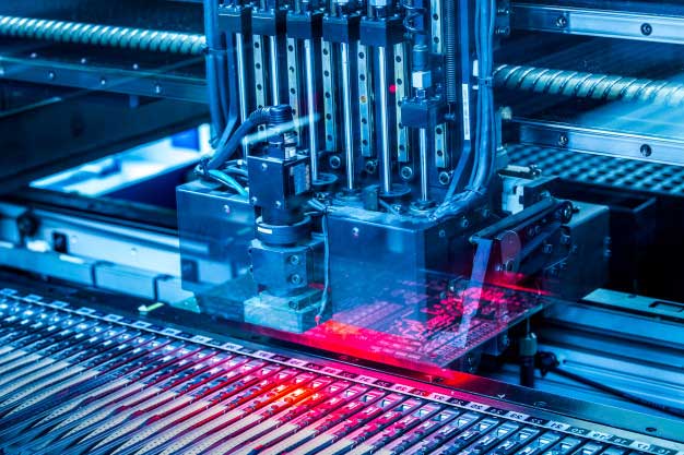
The process starts with laser direct imaging (LDI), which involves a laser beam used to create the desired pattern on the PCB’s surface. Next, an inkjet-printed layer is applied to the board before it is processed through the reflow oven. Finally, a solder mask is applied and cured, providing a protective coating to the finished product.

Legend printing ensures a superior level of quality for multilayer PCBs, giving designers the confidence to push the boundaries in their design requirements. With its combination of advanced technologies, it’s a reliable and cost-effective solution for producing complex electronic components. It also offers quick turnaround times with many fabrication capabilities, including small batch sizes and quick turnarounds. It’s no wonder why many leading companies rely on this cutting-edge technology to get them from concept to market quickly and efficiently. Moreover, if you’re looking for top-notch prototype PCBs, you can’t go wrong with legend printing.

Inkjet printing has many benefits that other processes cannot match. It provides a quick turnaround, allowing projects to go into production quickly, and allows designers to produce from a single-layer board or up to 10-layer boards. It helps make use of acid-free and water-based inks that deliver rich blacks, sharp text, high gloss finishes, and precise graphics. However, these advantages can increase the printing price. Like, an inkjet printer starts at about $10,000 and requires a costly startup investment. When these costs are factored in with maintenance fees, servicing needs, and running costs like ink replacement, this solution could prove to be too pricey for many companies.

The Multilayer PCB Manufacturing Process

Legend printing involves an advanced automated production system to ensure consistent and reliable results for customers. Generally, the process starts with a substrate, which consists of several layers of epoxy resin-bonded copper foil. Manufacturers then use imaging equipment to print the design onto the substrate and etch away the excess copper.

Then, they apply a layer of insulation material over the etched copper layer, followed by the insertion of conductive vias which electrically connect the layers. Finally, a solder mask is applied to protect the board from any accidental damage.

Through a multilayer PCB manufacturing process, you can produce intricate designs with high levels of accuracy and repeatability. This helps to ensure that your product will perform as expected when it reaches its final destination. The versatility of a multilayer PC BOARD manufacturing process also means that you can work on a wide range of different products.

Some industries that use legend printing include automotive, telecommunications, and aerospace applications. Each of these markets demands unique requirements and specifications, but they all require reliability and dependability. To keep up with the demands of each industry, we have developed innovative solutions through our experience in research and development. For example, aircraft are very sensitive structures, so some companies offer low-volume and pre-production testing services using the RISC or a rapid prototyping service. With such a service, you can reduce the lead times for tooling; maintain quality control during assembly, and reduce the risk exposure during the production ramp-up time.

The Benefits Of Legend Printing

The Legend printing-multilayer PCB manufacturing process offers several benefits for businesses looking to create complex circuit boards. By using this process, industries can ensure very high quality and accurate production.

The first benefit of using this process is that it allows for smaller board components. By using a multilayer system, more complex circuits are easy to create on smaller boards. This makes the boards easier to package and transport, saving the companies time and money.

Moreover, by using the legend printing-multilayer PCB manufacturing process, businesses can produce boards with superior electrical performance. This process can achieve high levels of precision and accuracy, leading to fewer errors and better overall performance.

Finally, this process allows for faster turnaround times. By utilizing multiple layers of production, businesses can quickly assemble complex circuits and get their products to market faster. This ensures that companies remain competitive in their industries and are able to capitalize on market trends quickly.

Overall, the Legend printing-multilayer PCB manufacturing process is an excellent option for businesses looking to maximize efficiency and quality when creating complex circuit boards. By utilizing this process, you are confident that your products are of the highest quality and are produced as quickly as possible.

Why Choose Legend Printing For Your Multilayer PCBs?

When it comes to designing and manufacturing multilayer PCBs, choosing the right manufacturing process is essential. Legend printing is a leading provider of multilayer PCBs, offering a comprehensive range of services that can help you get the most out of your multilayer PCBs.

The best legend printing companies use state-of-the-art equipment and processes to ensure quality, reliability, and performance. Our advanced Circuit board fabrication process starts with a detailed design and layout phase, allowing us to create high-quality multilayer boards with accurate dimensions.

Expert engineers use advanced manufacturing techniques and equipment to fabricate the boards. After production, they subject each board to a rigorous quality assurance process to guarantee that it meets all of your specifications.

The result is a multilayer PCB that is reliable and performs as expected in any application. Engineers also use advanced testing and inspection techniques to ensure that every product is up to high standards of quality and performance. By hiring a good printing company, you can trust that your multilayer PCB will be delivered on time and meet all of your requirements.

What To Consider While Making Legend Prints

You have to consider a few things during legend printing, be it new or some modifications, such as:

  • Texts should have the same orientation in the entire board, like reference designator, part numbers, brand details, etc. You should arrange the text from top to bottom.
  • Manufacturers often have to deal with overlapping texts that need editing. You can avoid it by moving the reference designator to the right side.
  • Though you can add legend printing on both sides of the board, it becomes expensive. So, you can reduce the cost by using only one side.
  • Markings should have standard shapes and colors to have readable and low-cost printing.
  • You can reduce printing faults through measurements. Keeping the space a few mils can reduce the errors.
  • Avoid placing text in four directions as it can make repair complex.
  • The text should not overlap the holes or vias, or it will lose its significance.
  • Try not to write the text on the fast signal paths, as it can cause dielectric loss, affecting the impedance level.

Legend printing involves different text styles, depending on the circuit board manufacturer and customers. Designers should check the styles before sending the Gerber files to fabricators.

Final Thoughts

Legend printing is a specialized multilayer PCB manufacturing process that combines the benefits of advanced technologies such as laser direct imaging and inkjet printing to produce high-quality printed circuit boards. The process creates layers of fine traces on the PCB, allowing for a high level of detail and accuracy, along with excellent signal integrity. You have to consider certain things during legend printing.

The legend printing-multilayer PCB manufacturing process is an excellent option for businesses looking to maximize efficiency and quality when creating complex circuit boards. By utilizing this process, you are confident that your products are of the highest quality and are produced as quickly as possible. If you’re looking for a reliable and cost-effective solution for your multilayer PCB needs, then look no further than legend printing.

Would like to know more about legend printing or PC Board assembly? Email us at sales@pnconline.com.

Printed Circuit Board

Printed Circuit Board Heat Sink Features/Functions

Heat management is essential for living on this earth as weather and devices affect buildings, vehicles, and equipment. Thermal management is also necessary for printed circuit boards, as they will get damaged if they can’t dissipate the heat their components generate. Besides, the board also gets hot due to soldering during manufacturing. Hence, heat dissipation methods become mandatory to increase the PCB speed.

Though FR4 is good at heat management, sometimes it is not enough when there is a high-speed circuit board. Likewise, the power supplies also generate heat and you have to install heat sinks and insulators. You must have experienced mechanical engineers to assess the heat flow to create a suitable heat dissipation system.

Printed circuit boards provide current to help devices function, but electronic devices get hot and heat sinks dissipate unnecessary heat. A PCB Manufacturer will use different heat sinks to prevent the overheating of PCB components and their damage, increasing the performance of the board.

Fourier’s law is an important law of heat that determines the heat sink function. When an element gets hot, heat travels from high-temperature areas to a low- temperature surface. The heat transfer occurs in three ways, such as:

  • Conduction
  • Radiation
  • Convention

When two components having different temperatures connect, it results in thermal conduction. In other words, fast molecules collide with slow molecules, resulting in heat transfer from hot components to cool components. PCB has high-temperature components like transistors, so you need to dissipate heat to cooling mediums, like water, air, or it can be oil, or some other element. This heat transfer occurs through conduction and convention.

Types of Heat Sinks

Heat sinks come up in different types as below:

Active Heat Sinks: There is a fan in an active heat sink to provide cooling. Such a heat sink provides great cooling, however, it needs regular maintenance as it is mostly running which affects its condition.

Passive Heat Sink: Passive heat sink is without a fan, so it remains still and needs less maintenance. You can consider it reliable and more effective than an active heat sink.

The shape and design also determine the type of heat sink, including swaged, stamped heat sinks, machining, folded and bonded fin, single fin sink, and forged heat sink.

Factors Affecting a Heat Sink

The main purpose of the heat sink is to exchange heat, so a large part of its surface area should be in contact with the cooling component like air. The quality of the heat sink depends on different factors, including its material, finishing, and certain physical features, like:

  • Air velocity
  • Attachment technique
  • Protrusion type

    Materials That Enhance Heat Sink Function

Manufacturers use specific materials to enhance the function of the heat sink in terms of heat transfer. These materials include:

  • Compounds
  • Conductive tape
  • Thermal paste

These materials are inserted between the surface of the heat sink and the surface of the component that generates heat. Metals having high thermal conductivity are ideal for heat sinks, including aluminum, copper, etc. But, aluminum is common as it is cheaper than others.

What To Consider Regarding Heat Sinks

Many factors affecting heat sink function include length, fin spacing and density, width, airflow, heat resistance, etc.

Which Devices Need Heat Sinks?

Electronic devices with components having poor heat dissipation ability need heat sinks. The devices in this case include multiple integrated circuits, diodes, transistors, switching devices, CPU and graphic processors, and LEDs.

Key Factors of Heat Sink Design

Heat sinks dissipate heat with the help of natural and forced convection, liquid, or radiation. The requirements of thermal management vary, depending upon the applications. Apart from a heat sink design, you have to consider several other factors while designing a thermal management system for a specific device. For like, you have to consider the standards of the component level, heat sink level standards, chassis levels, and requirements for a system level.

Let’s discuss essential factors that you have to consider during heat sink PCB design.

Heat Resistance: Thermal or heat resistance is the sum of multiple resistances occurring to heat flow between a cooling liquid and the die, thermal interference resistance, as well as the resistance between a moving fluid and a heat sink. Thermal resistance is bad for thermally unstable modeling systems.

The Value of Thermal Resistance: It is not precise, instead, it is approximate. It helps evaluate the thermal conductivity of the heat sinks and semiconductors. Heat dissipation depends on heat sink parameters that need proper analysis while designing the heat sink device. Heat sinks can be meshed through a 3D thermal resistance to have a complex system of thermal factors. Different platforms help design heat sink meshes.

Heat Sink Materials:  Generally, copper and aluminum are ideal heat sink materials as described above. These materials are good at conducting heat, especially copper as it also helps absorb heat, resists rust, and resist biofouling, moreover, it is also antimicrobial resistant. Though copper is better than aluminum, it is thick and costly compared to aluminum.

Another material is diamond and its thermal conductivity is also high due to the lattice vibrations it has. Some other materials for thermal applications include copper-tungsten pseudo-alloy, and AlSiCDymalloy.

Size and Shape of Heat Sink:  The shape and the size of the fins also help enhance heat dissipation. You can evaluate various fin shapes through modeling.

Fin Placement or Location: The arrangement of fins in a heat sink affects its cooling quality. Its configuration should be optimized to minimize the resistance of fluid movement, providing maximum air in the heat sink.

Cooling Quality: The cooling quality of the heat sinks has to be high. The aspect ratio of fins should be less to perform well. If the distance of the fin from the heat sink base is more, it will reduce the heat transfer to a cooling medium.

The function of the fins in a heat sink is to absorb heat from the electrical components of a device and sends it to the cooling medium. Besides, you should choose a cooling medium matching a PCB design and device requirements.

Heat Dissipation: Certain factors reduce the heat sink performance like a rough surface and gaps. They cause high resistance to thermal contact, thus affecting heat dissipation. You can reduce such thermal resistance by using thermal interface materials because most resistance-reduction techniques have limitations. You should consider specific things while selecting a thermal interface material, such as contact pressure, the material’s resistivity to current, and the dimensions of the surface gaps.

Attachment Methods: The attachment of the heat sink with PC Board components affects its thermal efficiency. So, you should choose the attachment technique carefully, considering the requirements of a thermal management system in terms of mechanical and thermal properties. Some popular attachment techniques include,

  • Thermal tape
  • Standoff spacers
  • Flat spring clamps

However, these attachment methods don’t end here as there are many others. You would also see m rein the future as engineers continuously update these methods according to new technologies.

By considering the above factors, engineers can design an effective heat dissipation system, including a heat sink.

Frequently Asked Questions

What Is Heat Sink?

The heat sink is a device and a way to manage heat in electronic products. Electronic components like transistors release heat, and you need heat sinks to dissipate heat to cooling mediums, like water, air, or it can be oil and other elements.

Do All Electronic Devices Need Heat Sinks?

Most devices need heat sinks to dissipate heat to cooling components. However, some electronic components have a built-in ability to dissipate heat. Generally, lasers or power transistors can’t transfer heat and need a solution to manage heat. MOSFETs and IGBTs are good examples in this case. So, here you need a heat sink device. 

Can PCB Survive Without Heat Sinks?

PCB components release heat which can damage them, making the electronic device slow. However, it also depends on the PCB materials as some have their heat dissipation property. Mostly you need a cooling system to enhance PCB performance. 

What Are The Types Of Heat Sinks?

The basic types in this case include the active heat sink system and the passive heat sink system. Some other types are also popular, like swaged heat sinks, stamped heat sinks, machining, folded and bonded fin, single-fin sinks, and forged heat sinks. 

Which Factors Influence The Heat Sink Design?

Many factors affect heat sink design, including its material, fin shape, and performance, fin size and location fin configuration, attachment technique of heat sink, and finally the thermal interface.

Final Thoughts

Devices having PCB also have heat sinks because they get hot due to high temperatures caused by different components. Heat sinks are either active or passive. You have to consider a few factors while designing the heat sinks, like its material, fin shape, and performance, fin size and location fin configuration, attachment technique of the heat sink, and finally the thermal interface. Various models help determine the heat sink parameters and geometry to provide a high-level heat transfer.

Would like to know more about the Heat Sink Features and Functions or pcb assembly services? Just Email us at sales@pnconline.com

TOTAL-CONCEPT

Total Concept Company

PNC’s expertise in design, manufacturing printed circuit boards, PCB assembly, and Box builds in one 70,000 sq./ft. facility makes us the ultimate total concept company. PNC’s unique manufacturing facility is just that, a PCB assembly usa manufacturer located in Nutley, New Jersey. PNC has been a vital supplier of electronics in the PCB industry for over 50 years and serves the military/defense, medical, aerospace, automotive, RF/Microwave, industrial and consumer sectors. Having these capabilities all in-house stream lines the turnkey process under one PO which is invaluable to our customers.

ELECTRONIC DESIGN

Being able to design in-house has its importance when designing for PCB manufacturing as well as prototype pcb assembly and production PCB assembly. Our designers have an edge in designing for PCB manufacturing since they are knowledgeable of the PCB manufacturing process. Designing for manufacturability eliminates defects, delays and process issues. Our design tools used are Cadence Allegro, OrCAD Capture, OrCAD PCB Designer and PADS. Our deliverables are Gerber, drill files, PCB File, schematics, Assembly and fabrication files and Formal drawings on customer format.

Having the capability to manufacture printed circuit boards, pcb contract manufacturing, in the same facility also has its benefits for prototype pcb assembly and production PCB assembly. While the printed circuit boards are in process of being fabricated, our pcb assembly division can work in parallel creating pick & place data, SMT Stencils, work instructions, AOI programing, selective soldering programming, and pre-pare testing procedures to expedite the PCB’s once the hit the SMT assembly floor. The work in parallel process makes for an efficient seamless transition from PCB manufacturing to Assembly.

TOTAL-CONCEPT-PCB
TOTAL-CONCEPT-PCB

After the PCB’s clear final inspection, they are transferred to the PCB assembly department. For a pcb assembly manufacturer in a total concept configuration, logistically you gain 1-2 days shipping time, since you do not have to outsource the PCB’s as well as a time savings of not have to perform an incoming inspection. PNC’s Assembly division is comprised of multiple high speed SMT lines with 13 zone re-flow ovens, 3d AOI, 3D X-ray, thru-hole stations, selective soldering, and rework stations. If required, PNC can perform Flying probe, ICT and functional testing to ensure a robust and error free PCBA.

Another SMT assembly service with-in our total concept company is box building. The PCB assembly never leaves the facility eliminating any ESD issues from incoming inspection handling. Our expertise in box building varies from small plastic snap together housing, medium sized metal enclosures to rack builds. If provided with a system test procedure, PNC testing engineers and technicians can perform the functional and burn in testing. When looking for total concept printed circuit assembly companies, we are here to help.