Tag Archives: pcb board assembly

PNC’s step by step guide to PCB Design component placement

A schematic is an abstraction, a representation of an ideal circuit. A PCB Assembly, on the other hand, is a complex mechanical assembly. All the components in the circuit design must fit within the physical boundary of the PCB. The designer must locate and place hundreds of components subject both to the mechanical constraints of the product design and the manufacturing process while not introducing electrical noise into the circuit.

It can seem overwhelming to someone new to the PCB layout process. Fortunately, there are some simple guidelines used by the designers at PNC that will help break the layout task into manageable pieces.

Initial component placement considerations

Start by identifying the mechanical constraints on the component location. The Printed Circuit Board size and shape will be defined by the overall product configuration. Typically, the product’s mechanical design will define the location of the connectors, the keep-out zones and the locations of the heat sinks. The initial mechanical layout of the PCB is often an iterative process defined during design and early prototyping.

One recommended keep-out area is the perimeter of the board. The perimeter should be kept free to give the manufacturer a place to grip the PCB during assembly process, and room to score smaller boards to allow them to be removed from a larger multi-arrayed panel.

PNC recommends that all components be kept .050” from the PCB edge. Taller and more fragile components like capacitors should be kept .125” from the edge if possible, to allow room for tooling access to prevent damage when the PC Board is routed or scored from the panel.

The next step is to divide the PCB into functional modules to simplify routing and grounding. This will help minimize noise between power components, high speed digital components and analog components. Switching power supplies are particularly noisy, so the power supplies and their associated components should be grouped together as far as possible from noise sensitive sections of the circuit. While defining the location of the modules, be aware that high power components will need heat sinks, which may limit placement options.

Locating active components

Once the edge components are placed and functional areas of the Printed Circuit Board are defined, the next step is to locate the BGAs, quad packs and other large high pin count components. The room needed to fan out their pin counts is going to drive the locations of all the components around them.

In general, try to align the active components ICs with the #1 pin or A1 pin in the same orientation. While this may not have any utility in the actual circuit, it will make inspection and debugging of the initial prototypes far less frustrating.

Locating passive components

As a follow on to locating the active components, the bypass or decoupling capacitors on the power pins should be located as close to the IC as practical to minimize the parasitic inductance. If more than one capacitor is being used PNC recommends that the lowest value capacitor should place closest to the power pin. If components will be located on both sides of the PC Board, the bypass capacitors are often located on the opposite side, directly under the power pin. If possible, each power pin should have its own bypass capacitor.

Polarized components such as electrolytic capacitors and diodes should be arranged so they are all facing the same way. During debugging, it is much easier to spot the one diode that is not like the others rather than having to look at the silkscreen of each diode to determine if it is installed correctly.

Pull-up resistors and other groups of identical components are often grouped and lined up to simplify layout, debugging and inspection. Consider using resistor arrays when possible to save board space and reduce component count.

Inductors break this placement guideline. Because inductors generate magnetic fields, placing them too close together, particularly end to end, can cause inductive coupling, changing the value of the inductors.

Layout of double-sided boards

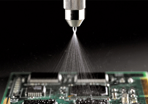
Double sided PCBs, PCBs with components on both sides, are expensive to produce, but may be necessary when real estate on the PCB design is tight, and when the overall product form factor is more important than PCB cost. A double-sided PCB is more expensive because it will need to pass though the pick and place machine and reflow oven twice.
Since the double-sided PCB will need to pass through the reflow oven twice, PNC recommends that the lighter and more heat resistant components be placed on the bottom of the board. Larger components on the bottom of the board will be glued to keep them from falling off, the smaller passive components cannot be glued, but the surface tension of the solder will hold them in place during the second pass through the oven.

Schedule a Design Review with your PCBA manufacturer

These are some general guidelines to aid in component placement used by the PCB designers at PNC. However, they are just guidelines. The best way to ensure that the printed circuit board assembly can be manufactured reliably is to have the layout reviewed by the people who will manufacture it. PNC’s designers can review your design to help reduce production cost and improve yield and reliability. Contact PNC today to schedule a review.

CONFORMAL-COATING

CONFORMAL COATING

What is Conformal Coating?

Conformal coating is protective chemical material coating applied after the final SMT PCB assembly or through-hole assembly process. Coatings are comprised of 5 different types, Acrylic, Epoxy, Urethane, Silicone and Parylene resins. Applying the coatings to a PCB board assembly can be done by hand spray, robotic spray, brush or dipping. The coating acts as an additional dielectric layer that provides protection due to environmental and mechanical stresses, such as thermal extremes, chemicals, dust, salt fog, abrasions, and moisture. In a PCB assembly that has close spacing of conductive pathways or close spacing of components the coating will help minimize dendrite growth over a period of time that causes shorting.

conformal_coating

Robotic Spray vs Traditional applications:

The method of application will depend on the customer requirements of the turnkey pcb assembly, but PNC prefers spray method for consistency in overall coating thickness. There are often select components on a pcb board assembly that will not be required to be coated. The traditional way is to block out or mask the selected components with tape. This is time consuming, costly and a possibility that the component can be damaged on the SMT assembly when removing. The robotic method can be programmed accurately to spray around the parts thus ensuring no component damage from masking and maintain a repeatable coating thickness.

When choosing a conformal coating for your turnkey pcb assembly, there are many manufacturers to choose from. The following are a few that we work with, Dymax, HumiSeal, Dow Corning, Hysol, Loctite, and Huntsman. Based on your application and environment of your PCB assembly, choose the Type of coating that fits the PCB board assembly, by visiting their web pages to find the strengths and weaknesses.

IPC J-STD-001D Conformal Coating thickness requirements

Type AR Acrylic Resin 0.03 – 0.13 mm (0.00118 – 0.00512 in)
Type ER Epoxy Resin 0.03 – 0.13 mm (0.00118 – 0.00512 in)
Type UR Urethane Resin 0.03 – 0.13 mm (0.00118 – 0.00512 in)
Type SR Silicone Resin 0.05 – 0.21 mm (0.00197 – 0.00827 in)
Type XY Parylene Resin 0.01 – 0.05 mm (0.000394 – 0.00197 in)

pcb manufactuter USA

Let PNC Simplify Your Printed Circuit Board Design With, CPLDs

New product designs continue to get more compact, while the performance and the number of features that customers expect continue to increase. To the engineer, this means higher PCB circuit densities and less room on the PCB for just-in-case design, such as unallocated I/O, or 0 ohm resistor networks to allow for reconfiguration of the PCBs at PCB assembly.

Meanwhile, new product prototype cycles are also getting faster. 3D printed mechanical parts are available within hours, putting pressure on electrical engineers to work faster and get their PCB designs right the first time. Even the fastest PCB fabrication, such as PNC’s 24-hour fabrication turn-time can’t help if the PCB has to be redesigned to fix errors.

The answer to both problems may be the CPLD. PNC’s CPLD programmers can help engineers reduce PCB size and allow on the fly circuit reconfiguration. Most people know that PNC specializes in fast PCB prototyping, but PNC is more than aPCB Manufacturer, PNC can speed prototyping by designing PCBs that replace inflexible circuit designs with PCBS that can be reconfigured to remap I/Os or change the order that circuit elements power up. A CPLD design developed by PNC can also allow the same PCB to be reconfigured to be used for the next generation product.

When it comes to programmable circuit elements, FPGA and microprocessors get all the good press. They are powerful, versatile, and generate more revenue for the manufacturers than workhorses such as CPLDS. Even though CPLD capability has improved dramatically over years, while both cost and power consumption have dropped, they are still often considered only for low level tasks such as “Glue Logic.” PNC designers can tell you that even a CPLD used for “low level” glue logic is appreciated when a late breaking design change means that two outputs now need to be two inputs, and one input needs to be inverted. All in a day’s work for PNC.

A PC Board Manufacturer, such as PNC can help you use these new, more capable CPLDs in places that can solve tough problems, replacing more expensive, complex and power-hungry solutions. Here are four examples.

I/O expansion

One of the most common CPLD applications is to expand the number of available microprocessor I/O ports. The CPLD I/O can either be multiplexed to the microprocessor or controlled via a serial interface. The advantage of a serial bus interface is that it allows you to locate this extra I/O anywhere, even on another Printed Circuit Board through a compact two or three pin connector.

The CPLD combinational logic architecture allows the creation of either a big fan-in or fan-out (over a hundred ports in some cases), and the outputs have enough current to drive small LEDS, a great way to create an array of circuit status LEDS.

When the CPLD output is used in conjunction with a CPLD’s internal clock the CPLD can also drive multiple PWM outputs allowing it to control things such as LED brightness, cooling fan speed, and simple sound producing devices.

The CPLD’s architecture gives it another useful capability for I/O expansion, the ability to accept inputs and drive outputs at different voltages. This multi voltage capability is often utilized for another common application; the communication bridge.

Bridges

CPLDs are often used as a bridge between one or more bus protocols, potentially at different voltages. They can support

  • serial to serial
  • serial to parallel,
  • parallel to parallel

They can even be used to drive an LCD. Because of their simple architecture, they have a low pin delay, making high speed synchronization possible.

Power Management

Another one of CPLD’s features is that they retain their programming and will boot within 500 µs. This means that the CPLD is the first programmable element to wake up on power up, so that it is awake and ready to manage the power up of power supplies and programmable devices ensuring they start in the right order.

Safety Systems

Because of the CPLDs simple architecture and 100% deterministic behavior CPLDs are often used in safety critical systems. One example application is to monitor interlocks, ensuring that the system is in a safe condition before the system can begin operation.

CPLDs pack a lot of capabilities into a compact package, they can reduce PCB complexity and allow reconfiguration on the fly. If you have never considered a CPLD in your design, the designers at PNC can help you with the CPLD circuit design, CPLD programming and Circuit board fabrication. Talk to PNC today.